Download
1 / 29
290 likes | 417 Views
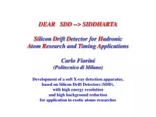
SIDDHARTA technical report. Mihai Iliescu on behalf of the SIDDHARTA collaboration. LNF SCIENTIFIC COMMITTEE 8-9 November 2004. Contents. SDD production Detectors mounting: ceramics and bonding Experimental setup Kaon trigger Front-end electronics Implementation plan.

E N D
SIDDHARTA technical report Mihai Iliescu on behalf of the SIDDHARTA collaboration LNF SCIENTIFIC COMMITTEE 8-9 November 2004
Contents • SDD production • Detectors mounting: ceramics and bonding • Experimental setup • Kaon trigger • Front-end electronics • Implementation plan
1.State of fabrication of large SDD array for the SIDDHARTA project (PNSensor, Munich) • Front side of the chip: electronic side with the drift rings fully finalized: implantationof the transistors; drift rings (including their intrinsic resistive connection); bulk contact; temperature diode; annealing • Deposition of protectingand isolating dielectric layers finalized within mid November • Back side of the chip: Back side structuring; implantation and annealing will start when the deposition of protecting layers of the front side will be finalized: first control measurements of leakage current performed at that moment • Nitride structuring within end 2004; aluminium deposition and structuringon the precursor wafers will startat the beginning 2005
1.State of fabrication of large SDD array for the SIDDHARTA project (PNSensor, Munich) • Electrical testing and cutting of the first wafers by the end of January 2005 • Dummy chips for supporting the substrate fabrication and testing the mounting and bounding issues already delivered to the Vienna group • 30 mm2 prototype chip delivered for testing to the Frascati group
sensitive area 3 x 100 mm² integrated temperature sensors SDD production status SDD layout – readout side chip size: 34 x 14 mm²
feedback capacitor inner substrate 150 µm source ring_1 reset diode R = 350 µm inner guard ring drain SDD layout – readout side, cell center • bond pads • 150 x 150 µm² • @ R ≈ 350 µm • 7 internal contacts • - source • - drain • - ring_1 • - inner guard ring • - inner substrate • - reset diode • - feedback cap. ~ 10 fF
Test in the laboratory of a 30mm2 SDD chip T = - 40°C, tsh=0.75ms
2. Detectors mounting: ceramics and bonding SDD bonding scheme – readout side
SDD-ceramic, bonding • Status: • 20 pieces of high purity prototype • ceramic boards are ready • first gluing test with SDD-dummies into • the high purity ceramic boards; • start of this tests mid of November • 2004, at the Fraunhofer Institute, • Berlin • cryogenic tests of the glued • SDD-dummy – ceramic board • at SMI, Vienna • perform first bonding tests with • SDD-dummies, to extract the • final working parameters • inspection of the bonding tests • at MPI-Halbleiterlabor, Munich • and SMI, Vienna
target cooling line feed-throughs for SDD electronics port for SDD cooling vacuum chamber SDD pre-amplifier electronics lead table SDD detector chip target cell beam pipe 3. Experimental setup
SDD mounting layout (Vienna group) cooling target cell pre-amplifier and voltage supply boards SDD cryogenic mounting device beam pipe
100 mm Cryogenic target cell (prototype) Status: Prototype under construction at SMI, Vienna target cooling SDD window 50 µm kapton thin-walled aluminum body kaon entrance window 125 µm kapton
1450 ps (tdc3+tdc4)/2 [50ps/ch] 4.Kaon trigger (Frascati group) Time of flight spectrum in the DEAR kaon monitor DEAR baseline: 10.5 cm SIDDHARTA baseline: 5.0 cm
PMT Type Max. Voltage [V] Gain Anode Pulse Rise Time [ns] Electron Transit Time [ns] Transit Time Spread [ns] Philips XP2020 2500 4x10⁷ 1.5 30 0.55 Hamamatsu R4998 2500 5.7x10⁶ 0.7 10 0.16 Scintillator Material Peak Wavelength [nm] Rise Time [ns] Decay Time [ns] Attenuation length [cm] NE104 406 0.6 1.8 120 BC420 391 0.5 1.5 110 Timing resolution improvement:Selection of PMT and Scintillating Material A prototype equipped with 4 Hamamatsu R4998 PMTs shall be ready for testing within February 2005
3 1 2 6 4 5 Preliminary scintillator array topology (Monte Carlo simulation) beam pipe
Simulated Coincidence Pattern 1- 4 Entries 1- 5 Uncorrelated hits 2 - 4 1- 6 3 - 4 3 - 5 3 - 6 2 - 5 2 - 6 Slab pairs
Simulated kaons arrival time Pattern: 1.and.(4.or.5.or.6) TDC Slab 1 [ps]
SDD array: 7 x 5 mm2 chips Fluorescence X- rays Fe55 Scintillator e- beam from BTFExcited material Pb slab e.m. shower Sr90 Trigger tests on an array of 7 x 5 mm2 SDD chips at Frascati Beam Test Facility
Incident rate: 60 Hz on 7 channels => 8.5 Hz/channel a) # Trigger OFF (16 hours.) # Cu signal visible; # No asynchronous backg (55Fe and 90Sr) # Continuous background: - synchronous from primary beam # 5 Hz b) # Trigger OFF (20 min.) # Cu signal embedded in backg. # Structured asynchronous backg: - Mn Ka and Kb from 55 Fe # Continuous background: - synchronous from primary beam - asynchronous from 90 Sr source # 60 Hz c) # Trigger ON, 1 ms (~ 16 hours) # Cu signal visible # Structured asynchronous backg. completely cut; # Continuous background: - synchronous from primary beam # 5 Hz – as a)
Incident rate: 1000 Hz on 7 channels => 142 Hz/channel a) # Trigger OFF (18 min.) # Cu signal embedded in background # Structured asynchronous background: - Mn Ka and Kb from 55 Fe - Ni Ka and Kb excited from Sr90 # Continuous background: - synchronous from primary beam - asynchronous from 90 Sr source # 1000 Hz b) # Trigger ON 1ms (~ 13 hours) # Cu signal visible # Structured asynchronous background completely cut; # Continuous background: - synchronous from primary beam # 5 Hz
5. Front-end electronics (Politecnico Milano) Study of the stability of the SDD Problem of the current configuration: Relevant peak shift by changing the signal current. SIDDHARTA foresees high and time-varying background Solution: Use of the SDD-JFET system in a Charge Preamplifier configuration
Scheme with CSA for improved stability BLH C1 HV drain A1 External A1 adjustment for P/Z cancellation Rd Isignal Cstray Pre out CF R P/Z Shaper out fixed Detector chip FE chip • Charge preamplifier (CA), instead of source follower + voltage preamplifier, for better stability • Design issues: same resolution as conventional configuration, insensitivity to stray capacitances • of the connections (critical for CA), JFET drain high-voltage driving, ext. pole-zero adjustement • Same unipolar and bipolar shaping circuits as in the conventional configuration • Improved rejection of baseline shifts by means of suitable Baseline Holder
Results from simulations of the VLSI analog channel with Charge Preamplifer Cstray: 0-30pF Preamplifier rise time Shaper output with baseline restorer
6020 6000 5980 5960 Position Mn line (eV) Max expected background rate 5940 5920 5900 5880 0 200 400 600 800 1000 1200 1400 1600 1800 Rate (Hz) with charge amp without charge amp Gain stability measurements in the LNF laboratory with the charge amplifier
350 330 310 290 270 FWHM (eV) 250 230 210 190 170 150 0 200 400 600 800 1000 1200 1400 1600 1800 Rate (Hz) with charge amp without charge amp Resolution measurements in the LNF laboratory with the charge amplifier
I run layout (submitted on 15 August 2004, ready mid Nov. 2004) Charge preamplifier + shaper (0.6-0.8-1.5-3ms peak times) Source follower + voltage preamplifier + shaper (0.6-0.8-1.5-3ms peak times) Charge preamplifier + shaper (0.8-1-2-4ms peak times)
SDD Bias Voltage Controller to enhance detector gain stability • Prototype to be used on the • 30 mm2 SDD chip, under development at IFIN Bucharest • Characteristics: • Communication: USB 1.1 • DSP board (Analog Devices) • Two Programmable A/D, D/O loops: • 9010V (16 bit accuracy /20V) • 19010V (16 bit accuracy /20V)