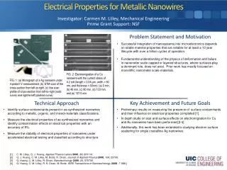
Download
1 / 27
280 likes | 534 Views
Wide Bandgap Semiconductor Nanowires for Sensing. S.J. Pearton 1 , B.S. Kang 1 , B.P.Gila 1 , D.P. Norton 1 , L.C.Tien 1 , H.T.Wang 2 , F. Ren 2 , Chih-Yang Chang 3 ,G.C. Chi 3 ,Wei-Ming Wang 3 and Li-Chyong Chen 4

E N D
Wide Bandgap Semiconductor Nanowires for Sensing • S.J. Pearton1, B.S. Kang1, B.P.Gila1, D.P. Norton1, L.C.Tien1, H.T.Wang2, F. Ren2, Chih-Yang Chang3,G.C. Chi3,Wei-Ming Wang3 and Li-Chyong Chen4 • 1Department of Materials Science and Engineering, University of Florida, Gainesville, FL 32611-6400, U.S.A • 2Department of Chemical Engineering, University of Florida, Gainesville, FL 32611, U.S.A. • 3Department of Physics, National Central University, Jhong-Li 320, Taiwan • 4Center for Condensed Matter Sciences, National Taiwan University, Taipei 106, Taiwan
GaN Applications • Blue/violet/white/UV LED Blue/green/UV lasers • High power microwave transistors • Robust sensors
500μm 5μm Ti/Au Pad SiNx/Si Ti/Au Pad FESEM image & CL spectrum of a single GaN NW with two electrodes
Gate voltage-dependent I-Vsd curves of a single GaN NW The carrier mobility is estimated at 30 cm2/V·s. The carrier concentration is estimated to be 2×1017 cm-3
InN NWs grown by catalytic thermal-CVD XRD spectrum HRTEM image
Resistivity comparison between thin film and nanowire (n-type GaN and InN)
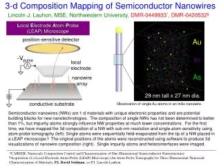
Single Crystal Nanowire 0002 0002 1010 1010 • TEM image of an individual ZnO Nanowire. • An estimated diameter of the wire is 20 nm. • A small particle embedded at the tip of the wire is Ag or Ag-Zn alloy. • HR-TEM image and selected area diffraction (SAD) of the nanowire indicates that it is a single crystal ZnO.
Sheath (Zn,Mg)O (Hexa.) (Mg,Zn)O (cubic) Core (Zn,Mg)O (Hexa.) Zn1-xMgxO (x <0.02) (Hexa.) Heterostructured nanowires Radial heterostructure Axial heterostructure Type I Type II ZnO (Zn1-XMgX)O ZnO (Zn1-XMgX)O Growth condition -. Zn : 3 × 10⁻⁶ mbar -. Mg : 2 × 10⁻⁷ mbar -. O3/O2 : 5 × 10⁻⁴ mbar, -. Tg= 400C Growth condition -. Zn : 3 × 10⁻⁶ mbar -. Mg : 4 × 10⁻⁷ mbar -. O3/O2 : 5 × 10⁻⁴ mbar, -. Tg= 400C
Sheath (Zn,Mg)O (Hexa.) Core (Zn,Mg)O (Hexa.) Type I - Radial heterostructured nanowire -. Nanowire is crystalline with the wurtzite crystal structure maintained throughout the cross-section. -. The higher contrast for the center core region clearly indicates a higher cation atomic mass. -. Core : zinc-rich Zn1-xMgxO -. Sheath : Mg-rich Zn1-yMgyO
a b b (Mg,Zn)O (cubic) Zn1-xMgxO (x <0.02) (Hexa.) 1120 0002 10 nm Type II - Radial heterostructured (Zn,Mg)O/(Mg,Zn)O nanowire Compositional line scan across the nanowire (STEM) (11ī) -. Core : Zn1-xMgxO Hexagonal Wurtzite structure -. Sheath (Shell): Mg1-xZnxO Cubic Rock salt structure Zn (1ī1) Mg (200) [0001]
Intensity(arb.) 2.04 Å Position across nanowire(nm) 020 200 B=[001] (Mg,Zn)O nanowire (cubic rock salt structure) Growth condition -. Zn : 3 × 10⁻⁶ mbar -. O3/O2 : 5 × 10⁻⁴ mbar, -. Mg : 8 × 10⁻⁷ mbar -. Tg = 400C
Nanowires vs Zn, Mg pressures Radial heterostructured (Zn,Mg)O (Mg,Zn)O ZnO I II hexagonal core / sheath core / sheath cubic (Zn1-xMgx)O/(Zn1-xMgx)O (Zn1-xMgx)O / (Mg,Zn)O wurtzite st. rock salt st. hexa. / hexa. hexa. / cubic wurtzite / wurtzite wurtzite / rock salt st. Zn = 3 × 10⁻⁶ O3/O2 = 5 × 10⁻⁴ Mg = none Zn = 3 × 10⁻⁶ O3/O2 = 5 × 10⁻⁴ Mg = 2 × 10⁻⁷ Zn = 3 × 10⁻⁶ O3/O2 = 5 × 10⁻⁴ Mg = 4 × 10⁻⁷ Zn = 3 × 10⁻⁶ O3/O2 = 5 × 10⁻⁴ Mg = 8 × 10⁻⁷ [unit: mbar] Tg= 400C
Fabrication of ZnO nanowire device ZnO Nanowire Motivation Electrode (Al/Pt/Au) Al/Pt/Au -. Fundamental understanding of transport -. Nanoelectronics -. Nano sensors (UV, chemical, bio.) Insulator Structure of Nanodevice -. Electrode : Al/Pt/Au by sputtering -. Diameter of ZnO nanowire : 130 nm -. Channel Length : 3.7 m
Prototype device fabrication sequence Find Nanowires Relative To Alignment Marks Deposit SiO2 Spin PMMA Resist Design and Deposit Alignment Marks E-beam Write Aligned Pattern And Develop Ethanol and Nanowire Suspension Deposit Metal And Lift Off Evaporation & Nanowires Deposition
on off UV Response of single ZnO nanowire UV 366nm at VD 0.25V UV 366nm Dark
Pt/ZnO nanowire Schottky Diode Pt/Au (schottky contact) Al/Pt/Au Al/Pt/Au Forward Bias Reverse Bias I=Io(eqV/nkT-1) Ideality factor = 1.1
Gate oxide ((Ce,Tb)MgAl11O19) Gate(Al/Pt/Au) Drain (Al/Pt/Au) Source (Al/Pt/Au) Nanowire Insulator (SiO2) Si Gate Oxide Source Drain Nanowire Depletion-mode ZnO nanowire field-effect transistor
Insulator (SiO2) Si pH Sensing with Single ZnO Nanowire electrode (Al/Pt/Au) Nanowire Microchannel
Hydrogen Detection • Hydrogen has been used as fuels in many NASA’s space exploration missions. • President Bush’s Hydrogen Fuel Initiative in 2003. • Why hydrogen sensing? • Safety! • Production, Storage, Transport • Hydrogen concentration in air reaches a dangerous level at 4%. ppm-level detection is needed.
Al/Pt/Au Al/Pt/Au Simple Fabrication Process • Direct deposition of metal contacts on the silicon substrate with nanorods. • No need to go through sonication and E-beam lithography to fabricate the sensors. • The sensor has better sensitivity (more nanorods combined).
Hydrogen-Selective Sensing at Room Temperature with ZnO Nanorods
Wireless Hydrogen Sensor System Prototype – powered by battery Remote Sensor Central Station Micro- controller Micro- controller 16x1 LCD RX Low-noise Op Amp TX 916 MHz
Self-Powered Wireless Sensor • Use energy from ambient • Solar, vibration, ambient RF radiation • Use energy supplied locally • Hydrogen flow, micro fuel cell, acoustic, thermal gradient • Use energy supplied remotely • Wireless power supply (wireless power transmission)
Conclusions • High quality,single-crystal growth of wide bandgap semiconductor nanowires • Bimodal growth of cored ZnO/(Zn,Mg)O heterostructured nanowires. • Type I -. Core : Zn1-xMgxO (x < 0.02) , Hexagonal wurtzite structure -. Sheath : Zn1-xMgxO (x >> 0.02), Hexagonal wurtzite structure • Type II -. Core : Zn1-xMgxO (x < 0.02), Hexagonal wurtzite structure -. Sheath : (Mg,Zn)O, Cubic rock salt structure • (Mg,Zn)O nanowires having cubic rock salt structure • Functional Nano-devices • Pt/ZnO nanowire Schottky Diode • Depletion-mode GaN and ZnO nanowire field-effect transistor • UV, pH, & gas sensors from GaN,InN and ZnO nanowires