Download
1 / 18
180 likes | 337 Views
Collaboration with Industry and Other Sectors. Summary of C-SPIN Partnerships Texas Instruments Collaboration International Collaborations Santos and Murphy - NTT and Tohoku Univ. (Japan) Salamo - Humboldt University (Germany)

E N D
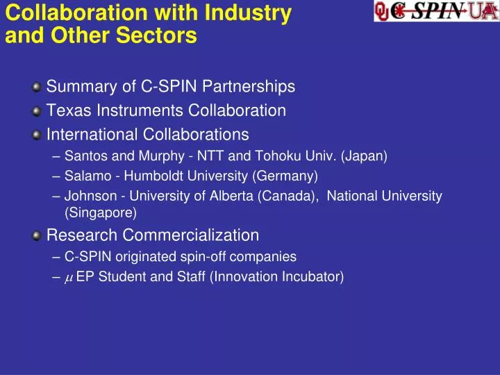
Collaboration with Industry and Other Sectors • Summary of C-SPIN Partnerships • Texas Instruments Collaboration • International Collaborations • Santos and Murphy - NTT and Tohoku Univ. (Japan) • Salamo - Humboldt University (Germany) • Johnson - University of Alberta (Canada), National University (Singapore) • Research Commercialization • C-SPIN originated spin-off companies • m EP Student and Staff (Innovation Incubator)
Selected Collaborations • Oklahoma • NTT and Tohoku University, Japan • Intel Corp. • IBM Burlington • IQE • Dupont • University of Alberta, Canada • Singapore National University • Sandia/ Los Alamos, CINT • Amethyst Research Inc., OK • Ekips/Phononics, OK • Arkansas • Texas Instruments • Army Research Laboratory • Air Force Research Lab • Quantum Dot Inc. • NanoSonic • Kodak • Kovio • Innovation Incubator Relevant Regional Activities • Oklahoma • OSU (materials) • OU (polymers, genome) • Nomadics Inc. (sensors) • Frontier Engineering (sensors) • Eagle-Picher (materials) • Phillips and Conoco (polymers) • Southwest NanoTechnolgies • Arkansas • UA (materials) • HiDEC (materials) • Genesis Technology Incubator • Integral Wave Technologies (passives) • Space Photonics (systems) • NN-Labs (materials)
Collaboration with Industry and Other Sectors • Summary of C-SPIN Partnerships • Texas Instruments Collaboration • International Collaborations • Santos and Murphy - NTT and Tohoku Univ. (Japan) • Salamo - Humboldt University (Germany) • Johnson - University of Alberta (Canada), National University (Singapore) • Research Commercialization • C-SPIN originated spin-off companies • m EP Student and Staff (Innovation Incubator)
Nanoferroelectric RAM: C-SPIN/TI Collaboration Research Collaboration Areas • Critical field calculations – Matching theory with experiment • MBE Growth of Ferro-electrics • Strain measurement within a PZT film (TEM) • Theory: multiferroics, ferro- electric & magnetic rings, dielectric susceptibility of nanostructures NSF/NRI Supplement to OU/UA MRSEC NSF/NRI Supplement: $50,000/yr Match: $50,000/yr Personnel Greg Salamo, PI– MBE Growth, AFM Characterization Matthew Johnson, PI (Physics, OU) – TEM Characterization Laurent Bellaiche, (Physics, UA ) - Theory and ferroelectric material design Post-Doc and Grad. Students. NRI Industrial Liaison Team Rick Wise, TI – Team Lead; Simone Raoux, IBM; Uday Udayakumar, TI-Dallas
Why FerroElectrics? • TIs Interest • FRAMs (Ferroelectric RAMs) are a non-volatile memory alternative. • TI’s use a lead zirconatetitanate (PZT) layer in the storage capacitor. • FRAMs are now on the market and will be incorporated into US “smart-passports” in the near future. • However, understanding of the PZT layer, especially within capacitor stack, is incomplete. • Need to look at existing PZT layers on the nanoscale with the TEM -TI’s earlier efforts unsuccessful. • Need to explore new growth techniques for FE materials, such as MBE. • Need to model FE materials to better understand behavior with scaling. • Overall Interest • Memory storage using ferroelectrics offer advantages over ferromagnetics, e.g. denser storage especially within toroidal geometries. • Possible devices that directly use FE materials e.g. ferroelectric field effect. • FE materials are a part of a bigger class of materials multi-ferroics have the potential to magneto-electric coupling. • Need to theoretically explore the behavior of ferroelectric and multi-ferroic nanostructures.
Key Progress • Critical Field / Temperature vs. Thickness • Calculated critical field & temperature (Ec, Tc) dependence on nanoferroelectric film thickness. • MBE Studies • SrO (BaO) and TiO2 grown as alternating layers on SrTiO3 substrates to make high-quality SrTiO3 (BaTiO3) epitaxial layers • TEM of FRAM Capacitors • For the first time we have used cross-sectional TEM image the crystal grains of the PZT layer within the capacitor stack. • Typical grain size: height = 67 ± 5 nm ; Width = 85 ± 27 nm • Orientation of grains obtained through Nano-Beam Diffraction (NBD) • Distinguish lattice parameter c from a using in situ calibration • Theoretical Studies: Multi-Ferroics & Dielectric Susceptibility of Nanostructures • Finite temperature properties of multi-ferroic structures • Hysteresis loops predicted in asymmetric, ferro- magnetic & electric rings • First-principle calculations & phenomenological theory suggest a dependence of external & internal susceptibilities to nanostructure shape & surroundings
MBE of BaTiO3 on SrTiO3 SrTiO3 (002) STO (100) substrate BaO layer on STO (100) TiO2 layer on STO (100) BaTiO3 (002) FWHM 680 arcsec High-Resolution X-ray Diffraction In situ RHEED patterns Grow monolayer of BaO then TiO2 etc. to obtain a BaTiO3 layer Shuttered RHEED Oscillation Curve XRD indicates excellent film quality. 180 loops: 1 hour 8 loops: 160 seconds
Embedded FRAM Data Storage • FRAM Nonvolatile Memory • Reduced total cost & power consumption vs Flash • But flash Tunnel oxide (SiO2 related) is simpler than PZT layers • Reduced magnetic susceptibility vs. MRAM • Will be in Passports PbZrxTi1-xO3 - Perovskite Ferro Cap Switching Characterization Data stored by switching ions between stable positions in PZT crystal. STEM showing PZT grains in a device capacitor.
c c c c c c c c 3 4 1 2 5 6 50 nm NBD Orientation of PZT Grains: Cap 6 (XT, YT)=(-3.8°, 2.4°) (-3.8° , 2.4°) (0.0° , 0.0°) (3.6° , 3.6°) • c-axis is preferentially oriented perpendicular to capacitor • Measured c/a ~ 1.02 -1.03 – indicating some strain in layer
Critical Field & Temperature vs. Thickness Critical temperature (Tc) is the temperature below which layer is ferroelectric (has remnant polarization). Critical field (Ec) is the field required to switch the polarization of the layer. For ultra-thin films these values depend on boundary conditions at the surfaces. Free-charge available (short circuit) or not (open circuit). Pb(Zr0.4Ti0.6)O3 Films, Compressive Strain 2.65%, T= 10K For short or open circuit, at a thickness of 40 or 50 nm Tc and Ecare the bulk values. APL 91, 152909 (2007) Phys. Rev. B 75, 085412, (2007)
Behavior of Asymmetric FE & FM Vortices a c d b Insets show the rings' geometry and the dipole arrangement in the (x,y) plane for eight important states: vortex states (1, 3, 5, & 7), onion states (2 & 4), and antiferrotoroidic pair states (6 & 8). Control of vortices by homogeneous fields in asymmetric ferroelectric (FE) and ferromagnetic (FM) rings: A unifying theoretical approach FerroMagnetic Rings FerroElectric Rings Predicted hysteresis loops in asymmetric FM rings (a,b) asymmetric FE rings (c,d). FM rings: (a,b) show the evolution of the magnetization and magnetic toroidal moment, vs. the applied homogeneous ac B-field. FE rings: (c,d) show the evolution of the polarization and electric toroidal moment, vs. the applied homogeneous ac E-field. Phys. Rev. Lett. 100, 047201 (2008)
Collaboration with Industry and Other Sectors • Summary of C-SPIN Partnerships • Texas Instruments Collaboration • International Collaborations • Santos and Murphy - NTT and Tohoku Univ. (Japan) • Salamo - Humboldt University (Germany) • Johnson - University of Alberta (Canada), National University (Singapore) • Research Commercialization • C-SPIN originated spin-off companies • m EP Student and Staff (Innovation Incubator)
MBE growth of InSb QWs at C-SPIN Device Processing at NTT & Hitachi C-SPIN Student at NTT, Japan B G G Hall bar with 50 mm channel Measurementsat NTT, Hitachi &C-SPIN I C Electron focusing device InSb Ballistic Transport Devices • Collaborative Projects • Laterally gated point contacts (NTT) • Magnetic focusing devices (NTT) • Extraordinary Magnetoresistance (Hitachi) • All involve industrial internships for students • Conference Presentations • APS March Meeting, 2002-2005 • Narrow Gap Semiconductors, 2003 • Modulated Semiconductor Structures, 2003 • Quantum Dots, 2004 • Electronic Properties of 2D Systems, 2005
Collaboration with Industry and Other Sectors • Summary of C-SPIN Partnerships • Texas Instruments Collaboration • International Collaborations • Santos and Murphy - NTT and Tohoku Univ. (Japan) • Salamo - Humboldt University (Germany) • Johnson - University of Alberta (Canada), National University (Singapore) • Research Commercialization • C-SPIN originated spin-off companies • m EP Student and Staff (Innovation Incubator)
Some C-SPIN start-ups • The mission of Nanolight, Inc. is to research and develop semiconductor nanofabrication techniques for implementation in cutting-edge infrared laser and detector systems and to assist others in their product development efforts by providing epitaxial-related services and acting as a distributor for nanofabrication equipment. • Founded in 2004 by Zhisheng Shi • $750K Phase 2 SBIR Grant to develop infrared technology for missile defense systems • $90K from OCAST to develop photoconductive mid-IR detector using an assembly of nanowires. • Ekips Technologies develops innovative laser-based sensors. Using technologies similar to those found in DVD players, these sensors will improve health care by enabling more effective point-of-care diagnostics. • Founded in 2000 by Patrick McCann • $350K from OCAST to develop four-level mid-infrared lasers with low power consumption and room temperature operation • Phononic Devices • Founded in 2008 by Patrick McCann • Develop IV-VI Thermoelectric Devices
More C-SPIN start-ups • Minotaur Technologies is a biophotonics company whose mission is to develop new laser-based instrumentation for life sciences research. The company is developing instruments that are applicable to a broad range of cell biology problems in neuroscience and beyond, including chemotaxis, stem-cell differentiation and in vitro testing of cellular response to emerging treatments. • Founded in 2003 by Min Xiao • Nanomaterials and Nanofabrication Laboratories (NN-Labs) focuses on production, processing and applications of semiconductor nanocrystals and dendron ligands. Since 2002 the company has received a multitude of Phase I and Phase II SBIR contracts from various government agencies to aid in funding the development of a wide range of nanocrystals and nanocrystal applications. • Founded in 2001 by Xiaogang Peng
http://www.nn-labs.com Patent licensing Existing Firms University Incubators • Conference Presentations • APS March Meeting, 2002-2005 • Narrow Gap Semiconductors, 2003 Highest quality Broadest wavelength range Large quantities Startup companies Local Economic Impact Invention (C-SPIN) Patent Rights (OU or UA) • Increase number of startup companies • Dramatic increase in SBIR grants
UA Innovation Incubator – I2 NSF Partnership for Innovation Program • Funded by a three-year, $840K NSF grant. • Spans m EP, Physics, College of Engineering, and the Arkansas Science and Technology Authority. • Performs proof-of-concept research for those interested in expanding or starting a small business.