Download
1 / 33
330 likes | 430 Views
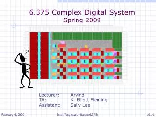
6.884 Complex Digital Systems Spring 2005. Lecturers: Arvind, Krste Asanovic TA: Christopher Batten Website: http://csg.csail.mit.edu/6.884/. Circuit Board: 8 / system 1-16G devices. Integrated Circuit: 8-16 / PCB 0.25M-1G devices. Module: 8-16 / IC 100K devices. MOSFET. Cell:

E N D
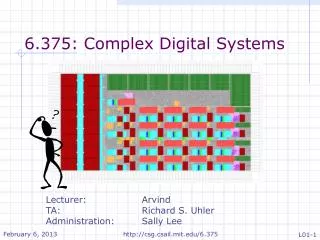
6.884 Complex Digital SystemsSpring 2005 Lecturers: Arvind, Krste Asanovic TA: Christopher Batten Website:http://csg.csail.mit.edu/6.884/
Circuit Board: 8 / system 1-16G devices Integrated Circuit: 8-16 / PCB 0.25M-1G devices Module: 8-16 / IC 100K devices MOSFET Cell: 1K-10K / Module 16-64 devices Scheme for representing information Gate: 2-16 / Cell 8 devices Modern Digital Systems Engineering Personal Computer: Hardware & Software
6.884 Objectives • By end of term, we expect you’ll be able to: • Select an economic implementation technology and tool flow: custom, cell or structured ASIC, ASSP, or FPGA • Decompose a top-level system requirement into a hierarchy of sub-units that are easy to specify, implement, and verify • Develop efficient verification and test plans • Select appropriate microarchitectures for a unit and perform microarchitectural exploration to meet price, performance, and power goals • Use industry-standard tool flows • Complete a working million gate chip design! • Make millions at a new chip startup (Don’t forget your alma mater!)
6.884 Prerequisites • You must be familiar with undergraduate (6.004) logic design : • Combinational and sequential logic design • Dynamic Discipline (clocking, setup and hold) • Finite State Machine design • Binary arithmetic and other information encodings • Simple pipelining • ROMs/RAMs/register files • Additional circuit knowledge (6.002, 6.374) useful but not vital • Architecture knowledge (6.823) helpful for projects
6.884 Structure • First half of term (before Spring Break) • Lectures and tutorials every MWF, 1pm-2:30pm in 24-307 • Around 3-5 labs hosted on Athena, lab machines in 38-301 • Form project teams (2-3 students) and prepare project proposal • Closed-book 90 minute quiz on last Friday before Spring Break • Second half of term (after Spring Break) • Each project team has scheduled weekly meeting with instructors • Weekly project milestones, with 1-2 page report due each week • Final project presentations in last week of classes • Final project report (~15-20 pages) due May 11 (no extensions) • Afterwards: • Possibility of fabricating best projects in 180nm technology • (summer+fall commitment)
6.884 Project • Two standard projects with fixed interfaces and testbenches: • MIPS microprocessor, team selects a design point: • High performance (e.g., speculative out-of-order superscalar) • Low power (e.g., aggressive clock gating, power-efficient L0 caches) • Minimal area (e.g., heavily multiplexed byte-wide datapath, compressed instruction stream) • Memory system, team selects a design point • Cache-coherent multiprocessor • Power-optimized memory system • Streaming non-blocking cache memory system • Custom project: • We will consider requests for non-standard project provided: • Group submits two-page proposal by March 11 • C/C++/Java reference implementation running by March 11 • Examples: MP3 player, H.264 encoder, Graphics pipeline, Network processor • Must work in teams of 2 or 3 students
6.884 Grade Breakdown • Labs (3-5): 30% • Quiz: 20% • Project milestones (5): 25% • Final project report: 25%
6.884 Collaboration Policy • We strongly encourage students to collaborate on understanding the course material, BUT: • Each student must turn in individual solutions to labs • Students must not discuss quiz contents with students who have not yet taken the quiz • If you’re inadvertently exposed to quiz contents before the exam, by whatever means, you must immediately inform the instructors or TA
What is a VLSI circuit? • VERY LARGE SCALE INTEGRATED CIRCUIT Technique where many circuit components and the wiring that connects them are manufactured simultaneously into a compact, reliable and inexpensive chip. Early (circa 1977) characterization of circuit “size” before people realized that the number of components per chip was quadrupling every 24 months (aka Moore’s Law)!
Dawn of the transistor Bell Labs lays the groundwork: 1940: Russel Ohl develops PN junction which produces 0.5V when exposed to light. 1945: Bell sets up lab in the hopes of developing “solid state” components to replace existing electromechanical systems. William Schockley, John Bardeen, Walter Brattain: all solid-state physicists. Focus on Si and Ge.1947: Bardeen and Brattain create point-contact transistor w/ two PN junctions. Gain = 18. Announced in July 1948. But treated as a novelty until 1951 invention of junction transistor. Bell Labs willing to license the rights to the transistor to any company for a royalty (which was waived for hearing aid companies as a gesture to Alex. G. Bell). Transistor was good: smaller, faster, more reliable and economical but this is only half the story since the circuits, albeit smaller, were still constructed in much the same way.
Dawn of the transistor (II) 1951: Shockley develops junction transistor which can be manufactured in quantity. 1952: GWA Dummer forecasts “solid block [with] layers of insulating, conducting and amplifying materials” 1954: The first transistor radio! Also, TI makes first silicon transistor (price $2.50) 1956: Bardeen, Shockley, Brattain receive Nobel Prize. (U.S. Patents #2,502,488, #2,524,035)
Early Integration (U.S. Patent #3,138,743) Jack Kilby was denied entry to MIT because of poor high school grades (went to U of I). Kilby worked on miniaturized components during the war and experimented with photolithography. Went to 1952 Bell Labs transistor course. High labor costs at TI got Kilby thinking about “solid circuits” over the July 1959 plant closing. Built phase-shift oscillator and it worked on 9/12/59. By the end of the year, he had constructed several examples, including the flip-flop shown in the patent drawing above. Components are connected by hand-soldered wires and isolated by “shaping” and PN diodes used as resistors. In December 2000, Kilby was awarded the Nobel Prize in physics for this work.
Making it real… (U.S. Patent #2,981,877) Robert Noyce experimented in the late 40’s with transistors while a physics major at college (his prof was friends with Bardeen at Bell and so had early access to transistors). He came to MIT where “much to his surprise, few people had even heard about the transistor.” After getting his PhD in 1953, he worked in industry, finally arriving at Mountain View, CA and Shockley Semiconductor Labs in 1955. In 1957, Noyce left Shockley’s lab (Schockley wasn’t the best of managers) to form Fairchild Semiconductor with Jean Hoerni. Gordon Moore is another founder. In early 1958, Hoerni invents technique for diffusing impurities into the silicon to build planar transistors and then using a SiO2 insulator. In spring of 1959, Kurt Lehovec at Sprague Elec. Co. here in North Adams, MA invents isolation technique using back-to-back pn junctions. In mid 1959, Noyce develops first true IC using planar transistors, back-to-back pn junctions for isolation, diode-isolated silicon resistors and SiO2 insulation wired using his innovation: using metal deposited by evaporation through a mask to form the interconnect -- keeping the IC flat and easy to build.
1960’s: Era of Integration (social and electrical!) 1961: TI and Fairchild introduced the first logic IC’s (cost ~$50 in quantity!). This is a dual flip-flop with 4 transistors. 1963: Densities and yields are improving. This circuit has four flip flops. 0.06” 0.038” 1966: Robert Dennard invents 1-T DRAM at IBM TJ Watson Research Center. 1967: Fairchild markets this semi-custom chip. Transistors (organized in columns) could be easily rewired using a two-layer interconnect to create different circuits. This circuit contains ~150 logic gates. Masks are laid-out, cut and checked by hand… beginnings of a design flow but no computer automation. 0.15”
“Moore Noyce” was trademarked for a hotel chain! INTegrated ELectronics = Intel 1968: Noyce and Moore leave Fairchild and found Intel. No business plan, just a promise to specialize in memory chips. They and Art Rock raise $2.5M in two days and move to Santa Clara. By 1971 Intel had 500 employees; by 1983 it had 21,500 employees and $1.1B in sales. 3mm 0.113” 4mm (U.S. Patent #3,821,715) In 1970, making good on its promise to its investors Intel (Joel Karp, Les Vadasz, John Reed) starts selling a 1K bit PMOS RAM, the 1103. It was a bear to interface to, but its density and cost make it the only game it town. Core memory dies… In 1971 Intel introduces the first microprocessor, designed by Ted Hoff. The 4004 had 4-bit buses and a clock rate of 108KHz. It had 2300 transistors and was built in a 10u process. It never captured much interest in the market and was soon eclipsed by its more capable brethren.
Exponential Growth Introduced in 1972, the 8008 had 3,500 PMOS transistors supporting a byte-wide data path. Despite its limitations, the 8008 was the first microprocessor capable of playing the role of computer CPU as demonstrated on the cover of the July ‘74 issue of Radio-Electronics. Last, but not least, on our tour is the 8080. Introduced in 1974, the 8080 had 6,000 NMOS transistors fab’ed in a 6u process. The clock rate was 2Mhz, more than enough to ignite the personal computer industry. At least Paul Allen and his partner thought so when they wrote a BASIC interpreter for the 8080 in 1975. They would later collaborate in another, more profitable, venture...
Moore’s Law… http://www.intel.com/intel/intelis/museum/exhibit/hist_micro/hof/hof_main.htm Shown with approximate relative sizes Intel 8086, 1978, 33mm2 10Mhz, 29K transistors, 3u Intel 80286, 1982, 47mm2 12.5Mhz, 134K transistors, 1.5u Intel 386DX, 1985, 43mm2 33Mhz, 275K transistors, 1u Intel 8080A, 19743Mhz, 6K transistors, 6u Intel 486, 1989, 81mm2 50Mhz, 1.2M transistors, .8u Intel Pentium, 1993/1994/1996, 295/147/90mm2 66Mhz, 3.1M transistors, .8u/.6u/.35u Intel Pentium II, 1997, 203mm2/104mm2 300/333Mhz, 7.5M transistors, .35u/.25u
IBM Power 5 • 130nm SOI CMOS with Cu • 389mm2 • 2GHz • 276 million transistors • Dual processor cores • 1.92 MB on-chip L2 cache • 8-way superscalar • 2-way simultaneous multithreading
Modern Application-Specific IC (ASIC) Multiple functional blocks (some general purpose) stitched together at the top level to make video encoder/decoder. Lots of modeling at architectural level to ensure that functional goals could be met. Different teams worked on the different blocks. Note that each block is itself composed of sub-blocks, and so on for many levels of hierarchy. Lots of iteration and reuse… Many different architectural choices: RISC controller, SIMD compute engine, special purpose motion estimator. Each choice made to meet some performance and area goal. Used lots of clever implementation tricks: the “obvious” implementation derived from the spec would require a chip many times this size (and hence impossible to build today). 2.5M transistors required lots of support from CAD tools for assembling the blocks, doing the routing and VERIFYING that everything was hooked up okay. AVP-III Video Codec from Lucent Technologies
ASIC Design Styles • Full-Custom (every transistor hand-drawn) • Best performance: as used by Intel uPs • Semi-Custom (Some custom + some cell-based design) • Reduced design effort: AMD uPs plus recent Intel uPs • Cell-Based ASICs (Only use cells in standard library) • This is what we’ll use in 6.884 • Mask Programmed Gate Arrays • Popular for medium-volume, moderate performance applications • Field Programmable Gate Arrays • Popular for low-volume, low-moderate performance applications • Comparing styles: • how much freedom to develop own circuits? • how many design-specific mask layers per ASIC?
Full Custom Design • Designer is free to do anything, anywhere • though each design team usually imposes some discipline • Most time consuming design style • Reserved for very high performance or very high volume devices (Intel microprocessors, RF power amps for cellphones) • Requires complete customization of all layers of wafer Piece of full-custom multiplier array, 1.0mm 2-metal
Custom and Semi-Custom • In most extreme case, every transistor instance can be individually sized • approach used in Alpha microprocessor development • Over time, trend towards greater use of semi-custom design style • use a few great circuit designers to create cells • redirect most effort at microarchitecture and cell placement to keep wires short • Usually, in-house design team develops own libraries of cells for various types of components: • memories • register files • datapath cells • random logic cells • repeaters • clock buffers • I/O pads • Critical pieces can always resort to full-custom circuit
Standard Cell ASICs • Also called Cell-Based ICs (CBICs) • Fixed library of cells plus memory generators • Cells can be synthesized from HDL, or entered in schematics • Cells placed and routed automatically • Requires complete set of custom masks for each design • Currently most popular hard-wired ASIC type (6.884 will use this) Cells arranged in rows Mem 1 Mem 2 Generated memory arrays
Standard Cell Design • Cells have standard height but vary in width • Designed to connect power, ground, and wells by abutment Well Contact under Power Rail Clock Rail (not typical) Clock Rail VDD Rail Cell I/O on M2 Power Rails in M1 GND Rail NAND2 Flip-flop
Standard Cell Design Examples Channel routing for 1.0mm 2-metal stdcells Over cell routing for 0.18mm 6-metal stdcells
Gate Arrays • Can cut mask costs by prefabricating arrays of transistors on wafers • Only customize metal layer for each design GND • Fixed-size unit transistors • Metal connections personalize design Two kinds: • Channeled Gate Arrays • Leave space between rows of transistors for routing • Sea-of-Gates • Route over the top of unused transistors NMOS PMOS VDD PMOS NMOS GND [ OCEAN Sea-of-Gates Base Pattern ]
Gate Array Personalization Isolating transistors with “off” gate Isolating transistors by shared GND contact GND
Gate Array Pros and Cons • Cheaper and quicker since less masks to make • Can stockpile wafers with diffusion and poly finished • Memory inefficient when made from gate array • Embedded gate arrays add multiple fixed memory blocks to improve density (=>Structured ASICs) • Cell-based array designed to provide efficient memory cell (6 transistors in basic cell) • Logic slow and big due to fixed transistors and wiring overhead • Advanced cell-based arrays hardwire logic functions (NANDs/NORs/LUTs) which are personalized with metal
Field-Programmable Gate Arrays • Each cell in array contains a programmable logic function • Array has programmable interconnect between logic functions • Arrays mass-produced and programmed by customer after fabrication • Can be programmed by blowing fuses, loading SRAM bits, or loading FLASH memory • Overhead of programmability makes arrays expensive and slow but startup costs are low, so much cheaper than ASIC for small volumes
Unit A Unit B Unit C Iterate to meet functionality, timing, power goals Combinational Logic Unit-Transaction Level (UTL) Shared Memory Clock 6.884 ASIC/FPGA Design Flow Manual Translation Register-Transfer Level (RTL) (Bluespec/Verilog) Map to ASIC Map to FPGA Gate-based Implementations
6.884 Course Philosophy • Design is central focus • Architectural design has biggest impact on development cost and final quality • Good tools support design space exploration • e.g., Bluespec • Good design discipline avoids bad design points • Unit-Transaction Level design to decompose upper levels of design hierarchy • “Best-Practice” microarchitectural techniques within units