Download
1 / 3
30 likes | 41 Views
Author: Viet Phuong Pham<br>The induced contaminations (e.g polymer residues or impurities in air) on nanomaterial surfaces have been a serious problem to probe their intrinsic properties and for unique applications in surface chemistry, electronic, and optoelectronic. The polymer residues still presented on chemical vapor deposited graphene surface after its wet transfer (e.g. poly(methyl methacrylate) (PMMA)) on the arbitrary substrates tends to cause problems such as electrical degradation and unwanted intentional doping. Polymer residues (e.g PMMA), defects, and other contaminations are commonly leaving the thin layers or the particles as residues on nanomaterials.<br>Edelweiss Applied Science and Technology is an open access journal, our journal has a wide scope of topics related to science and technology, which are not limited to Basic Science, life science, computer science, environmental science, chemical science, electrical science, electronic engineering, industrial engineering, material science, astronomy and astrophysics. <br>

E N D
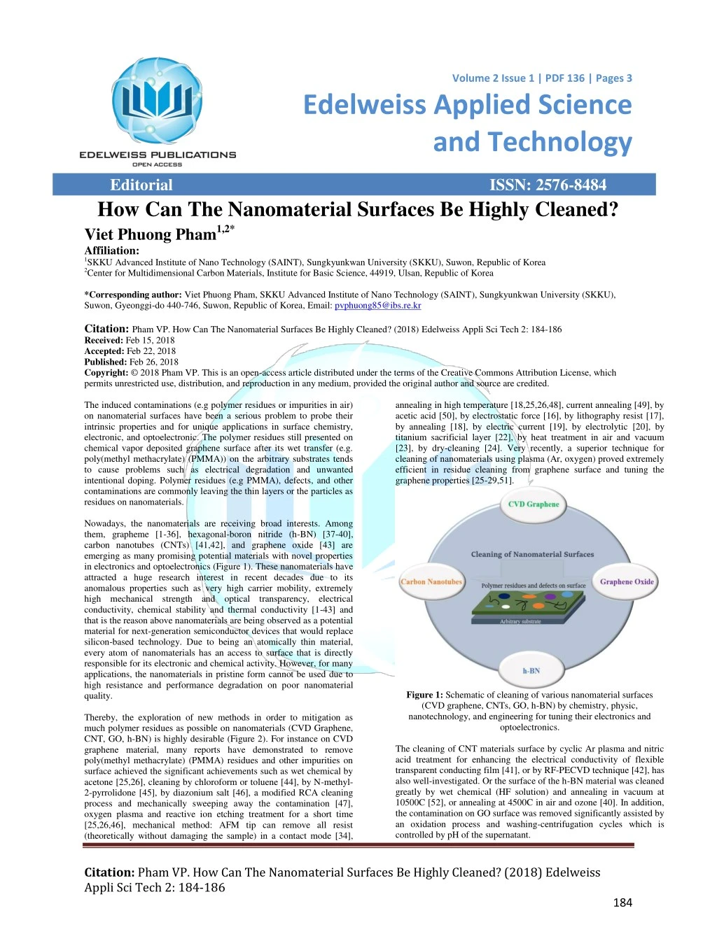
Volume 2 Issue 1 | PDF 136 | Pages 3 Volume 1 . Issue 1 | PDF 101 | Page 1 of x Edelweiss Applied Science and Technology Editorial How Can The Nanomaterial Surfaces Be Highly Cleaned? Viet Phuong Pham1,2* Affiliation: 1SKKU Advanced Institute of Nano Technology (SAINT), Sungkyunkwan University (SKKU), Suwon, Republic of Korea 2Center for Multidimensional Carbon Materials, Institute for Basic Science, 44919, Ulsan, Republic of Korea *Corresponding author: Viet Phuong Pham, SKKU Advanced Institute of Nano Technology (SAINT), Sungkyunkwan University (SKKU), Suwon, Gyeonggi-do 440-746, Suwon, Republic of Korea, Email: pvphuong85@ibs.re.kr Citation: Pham VP. How Can The Nanomaterial Surfaces Be Highly Cleaned? (2018)Edelweiss Appli Sci Tech 2: 184-186 Received: Feb 15, 2018 Accepted: Feb 22, 2018 Published: Feb 26, 2018 Copyright: © 2018 Pham VP. This is an open-access article distributed under the terms of the Creative Commons Attribution License, which permits unrestricted use, distribution, and reproduction in any medium, provided the original author and source are credited. The induced contaminations (e.g polymer residues or impurities in air) on nanomaterial surfaces have been a serious problem to probe their intrinsic properties and for unique applications in surface chemistry, electronic, and optoelectronic. The polymer residues still presented on chemical vapor deposited graphene surface after its wet transfer (e.g. poly(methyl methacrylate) (PMMA)) on the arbitrary substrates tends to cause problems such as electrical degradation and unwanted intentional doping. Polymer residues (e.g PMMA), defects, and other contaminations are commonly leaving the thin layers or the particles as residues on nanomaterials. Nowadays, the nanomaterials are receiving broad interests. Among them, grapheme [1-36], hexagonal-boron nitride (h-BN) [37-40], carbon nanotubes (CNTs) [41,42], and graphene oxide [43] are emerging as many promising potential materials with novel properties in electronics and optoelectronics (Figure 1). These nanomaterials have attracted a huge research interest in recent decades due to its anomalous properties such as very high carrier mobility, extremely high mechanical strength and optical transparency, electrical conductivity, chemical stability and thermal conductivity [1-43] and that is the reason above nanomaterials are being observed as a potential material for next-generation semiconductor devices that would replace silicon-based technology. Due to being an atomically thin material, every atom of nanomaterials has an access to surface that is directly responsible for its electronic and chemical activity. However, for many applications, the nanomaterials in pristine form cannot be used due to high resistance and performance degradation on poor nanomaterial quality. Thereby, the exploration of new methods in order to mitigation as much polymer residues as possible on nanomaterials (CVD Graphene, CNT, GO, h-BN) is highly desirable (Figure 2). For instance on CVD graphene material, many reports have demonstrated to remove poly(methyl methacrylate) (PMMA) residues and other impurities on surface achieved the significant achievements such as wet chemical by acetone [25,26], cleaning by chloroform or toluene [44], by N-methyl- 2-pyrrolidone [45], by diazonium salt [46], a modified RCA cleaning process and mechanically sweeping away the contamination [47], oxygen plasma and reactive ion etching treatment for a short time [25,26,46], mechanical method: AFM tip can remove all resist (theoretically without damaging the sample) in a contact mode [34], ISSN: 2576-8484 annealing in high temperature [18,25,26,48], current annealing [49], by acetic acid [50], by electrostatic force [16], by lithography resist [17], by annealing [18], by electric current [19], by electrolytic [20], by titanium sacrificial layer [22], by heat treatment in air and vacuum [23], by dry-cleaning [24]. Very recently, a superior technique for cleaning of nanomaterials using plasma (Ar, oxygen) proved extremely efficient in residue cleaning from graphene surface and tuning the graphene properties [25-29,51]. Figure 1: Schematic of cleaning of various nanomaterial surfaces (CVD graphene, CNTs, GO, h-BN) by chemistry, physic, nanotechnology, and engineering for tuning their electronics and optoelectronics. The cleaning of CNT materials surface by cyclic Ar plasma and nitric acid treatment for enhancing the electrical conductivity of flexible transparent conducting film [41], or by RF-PECVD technique [42], has also well-investigated. Or the surface of the h-BN material was cleaned greatly by wet chemical (HF solution) and annealing in vacuum at 10500C [52], or annealing at 4500C in air and ozone [40]. In addition, the contamination on GO surface was removed significantly assisted by an oxidation process and washing-centrifugation cycles which is controlled by pH of the supernatant. Citation: Pham VP. How Can The Nanomaterial Surfaces Be Highly Cleaned? (2018) Edelweiss Appli Sci Tech 2: 184-186 184
Pham VP. Edelweiss Applied Science and Technology, 2018 PDF: 136, 2:1 8. Pham VP. Chemical vapor deposited graphene synthesis with same- oriented hexagonal domains (2017) Eng. Press 1: 39-42. Kim KN, Pham VP, Yeom GY. Chlorine radical doping of a few layer graphene with low damage (2015) ECS J. Solid State Sci. Technol. 4: N5095-N5097. 10.Pham VP, Yeom GY. Recent advances in doping of molybdenum disulphide: industrial applications and future prospects (2016) Adv Mater 28: 9024-9059. 11.Ferrari AC, Bonaccorso F, Fal'ko V, et al. Science and technology roadmap for graphene, related two-dimensional crystals, and hybrid systems (2015) Nanoscale 7: 4587-5062. 12.Butler SZ et al. Progress, challenges, and opportunities in two- dimensional materials beyond graphene (2013) ACS Nano 7: 2898- 2926. 13.Geim AK, Novoselov KS. The rise of graphene (2007) Nat Mater 6: 183-191. 14.Zhang H, Yang P, Prato M. Grand challenges for nanoscience and nanotechnology (2015) ACS Nano 9: 6637-6640. 15.Kim KS, Ji YJ, Nam Y, Kim KH, Singh E, et al. Atomic layer etching of graphene through controlled ion beam for graphene-based electronics (2017) Sci. Rep. 7: 2462. 16.Choi WJ, Chung YJ, Park S, Yang CS, Lee YK, et al. A simple method for cleaning graphene surfaces with an electrostatic force (2014) Adv. Mater. 26: 637-644. 17.Ishigami M, Chen JH, Cullen WG, Fuhrer MS, Williams ED. Atomic structure of graphene on SiO2 (2007) Nano Lett. 7: 1643- 1648. 18.Lin YC, Lu CC, Yeh CH, Jin C, Suenaga K, et al. Graphene annealing: how clean can it be? (2011) Nano Lett. 12: 414-419. 19.Moser J, Barreiro A, Bachtold A. Current-induced cleaning of graphene (2007) Appl. Phys. Lett. 91: 161513. 20.Sun J, Finklea HO, Liu Y. Characterization and electrolytic cleaning of poly(methyl methacrylate) residues on transferred chemical vapor deposited graphene (2017) Nanotechnology 28: 125703. 21.Wood JD, Doidge GP, Carrion EA, Koepke JC, Kaitz JA, et al. Annealing free, clean graphene transfer using alternative polymer scaffolds (2015) Nanotechnology 26: 055302. 22.Joiner CA, Roy T, Hesabi ZR, Chakrabarti B, Vogel EM. Cleaning graphene with a titanium sacrificial layer (2014) Appl. Phys. Lett. 104: 223109. 23.Tripathy M, Mittelberge A, Mustonen K, Mangler C, Kotakoski J, et al. Cleaning graphene: comparing heat treatments in air and in vacuum (2017) Phys. Status Solidi RRL 11: 1700124. 24.Siller GA, Lehtinen O, Turchanin A, Kaiser U. Dry-cleaning of graphene (2014) Appl. Phys Lett. 104: 153115 25.Peltekis N, Kumar S, McEvoy N, Lee K, Weidlich A, et al. The effect of downstream plasma treatments on graphene surfaces (2011) Carbon 50: 395-403. 26.McEvoy N, Nolan H, Kumar NA, Hallam T, Duesberg GS. Functionalisation of graphene surfaces with downstream plasma treatments (2013) Carbon 54: 282-290. 27.Prudkovskiy VS, Katin KP, Maslov MM, Puech P, Yakimova R. Efficient cleaning of graphene from residual lithographic polymers by ozone treatment (2016) Carbon 109,: 221-226. 28.Hadish F, Jou S, Huang BR, Kuo HA, Tu CW. Functionalization of CVD grown graphene with downstream oxygen plasma treatment for glucose sensors (2017) J. Electrochem. Soc. 164: B336-B341. 29.Mumen HA, Rao F, Li W, Dong L. Singular sheet etching of graphene with oxygen plasma (2014) Nano-Micro Lett. 6: 116-124. 9. Figure 2: Cleaning process of various nanomaterial surfaces such as carbon nanotubes (a-c), graphene (d-e), h-BN (f,g), and GO (i,j). (a-c) reproduced with permission from [41]. (d,e) reproduced with permission from [17]. (f,g) reproduced with permission from [40]. (i,j) reproduced with permission from [43]. The cleaning of nanomaterials (CVD Graphene, CNT, h-BN, GO) using various strategies related to chemistry, physic, nanotechnology, and engineering in order to obtain the ultra-clean material layer and resulting in improving their electrical characteristics is highly desiring with targeting toward practical applications in the industry to serve human society. The enhancing of electrical properties of cleaned nanomaterials would be raising up the current on-off ratio, photoluminescence, and other unexploited and unexplored exotic properties. Consequently, it could unlock and take a leap forward on developing superior plasma-based cleaning methods [15,32], for other TMDs and low-dimensional materials in various advanced devices and applications. References 1. Novoselov KS, Geim AK, Morozov SV, Jiang D, Zhang Y, et al. Electric field effect in atomically thin carbon films (2004) Science 306: 666-669. Pham VP, Jang HS, Whang D, Choi JY. Direct growth of graphene on rigid and flexible substrates: progress, applications and challenges (2017) Chem Soc Rev 46: 6276-6300. Pham VP, Nguyen MT, Park JW, Kwak SS, Nguyen DHT, et al. Chlorine-trapped CVD bilayer graphene for resistive pressure sensor with high detection limit and high sensitivity (2017) 2D Materials 4: 025049. Pham VP, Kim KN, Jeon MH, Kim KS, Yeom GY, et al. Cyclic chlorine trap-doping for transparent, conductive, thermally stable and damage-free graphene (2014) Nanoscale 6: 15301-15308. Pham VP, Kim KH, Jeon MH, Lee S H, Kim KN, et al. Low damage pre-doping on CVD graphene/Cu using a chlorine inductively coupled plasma (2015) Carbon 95: 664-671. Pham VP, Mishra A, Yeom GY. The enhancement of Hall mobility and conductivity of CVD graphene through radical doping and vacuum annealing (2017) RSC Adv 7: 16104-16108. Pham VP, Kim DS, Kim KS, Park JW, Yang KC, et al. Low energy BCl3 plasma doping of few-layer graphene (2016) Sci Adv Mater 8: 884-890. 2. 3. 4. 5. 6. 7. Citation: Pham VP. How Can The Nanomaterial Surfaces Be Highly Cleaned? (2018) Edelweiss Appli Sci Tech 2: 184-186 185
Pham VP. Edelweiss Applied Science and Technology, 2018 PDF: 136, 2:1 30.Sun H, Chen D, Wu Y, Yuan Q, Guo L, et al. High quality graphene films with a clean surface prepared by an UV/ozone assisted transfer process (2017) J. Mater. Chem. C 5: 1880-1884. 31.Choi W, Shehzad MA, Park S, Seo Y. Influence of removing PMMA residues on surface of CVD graphene using a contact-mode atomic force microscope (2016) RSC Adv. 7: 6943-6949. 32.Kim KS, Hong HK, Jung H, Of IK, Lee Z, et al. Surface treatment process applicable to next generation graphene-based electronics (2016) Carbon 104: 119-124. 33.Jia Y, Gong X, Peng P, Wang Z, Tian Z, et al. Toward high carrier mobility and low contact resistance: laser cleaning of PMMA residues on graphene surfaces (2016) Nano-Micro Lett. 8: 336-346. 34.Goossens AM, Calado VE, Barreiro A, Watanabe K, Taniguchi T, et al. Mechanical cleaning of graphene (2012) Appl. Phys Lett. 100: 073110. 35.Choi H, Kim JA, Cho Y, Hwang T, Lee J, et al. Surface cleaning of graphene by CO2 cluster (2015) Solid State Phenomena 219: 68-70. 36.Kumar K, Kim YS, Yang EH. The influence of thermal annealing to remove polymeric residue on the electronic doping and morphological characteristics of graphene (2013) Carbon 65: 35-45. 37.Dean CR, Young AF, Lee C, Wang L, Sorgenfrei S, et al. Boron nitride substrates for high-quality graphene electronics (2010) Nature Nanotech 5 :722-726. 38.Elbadawi C, Tran TT, Kolibal M, Sikola T, Scott, et al. Electron beam directed etching of hexagonal boron nitride (2016) Nanoscale 8: 16182-16196. 39.Liao Y, Tu K, Han X, Hu L, Connell JW, et al. Oxidative etching of hexagonal boron nitride towards nanosheets with defined edges and holes (2015) Sci. Rep. 5: 14510. 40.Bueno JC, Cavalieri M, Wang R, Houri S, Hofmann S, et al. Mechanical characterization and cleaning of CVD single-layer h-BN resonators (2017) npj 2D materials and applications 1: 16. 41.Phuong VP, Jo YW, Oh JS, Kim SM, Park JW, et al. Effect of plasma-nitric acid treatment on the electrical conductivity of flexible transparent conductive films (2013) Jpn. J. Appl. Phys. 52: 075102. 42.Di H, Li M, Li H, Huang B, Yang B. Purification and characterization of carbon nanotubes synthesized by RF-PECVD (2012) ECS Trans. 44: 499-504. 43.Barbolina I, Woods CR, Lozano N, Kostarelos K, Novoselov KS, et al. Purity of graphene oxide determines its antibacterial activity (2016) 2D Materials 3:025025. 44.Niranan P, Marco S, Alberto D, Athanasia A. Effect of solvents on the dynamic behavior of poly(methyl methacrylate) film prepared by solvent casting (2011) J. Mater. Sci. 46: 5044-5049. 45.Xuelei L, Brent AS, Irene C, Guangjun C, Christina AH, et al. Toward clean and crackles transfer of graphene (2011) ACS Nano 5: 9144-9153. 46.Xiao YF, Ryo N, Li CY, Katsumi T. Effects of electron-transfer chemical modification on the electrical characteristics of graphene (2010) Nanotechnology 21: 475208. 47.Stephen C, Peter RK, Preston JR. Nanoimprint lithography (1996) J. Vac. Sci. Technol. B 14: 4129-4133. 48.Wei SL, Chang TN, John TLT. What does annealing do to metal- graphene contacts? (2014) Nano Lett. 14: 3840-3847. 49.Moser J, Barreiro A, Bachtold A. Current-induced cleaning of graphene (2007) Appl. Phys. Lett. 91: 163513. 50.Michael H, Ryan B, Lukas N. Graphene transfer with reduced residue (2013) Phys Lett. A 377: 1455-1458. 51.Lim YD, Lee DY, Shen TZ, Ra CH, Choi JY, et al. Si-compatible cleaning process for graphene using low-density inductively coupled plasma (2012) ACS Nano 6, 4410-4417. 52.King SW, Nemanich RJ, Davis RF. Cleaning of pyrolytic hexagonal boron nitride surfaces (2015) Surf. Interface Anal. 47: 798-803. Citation: Pham VP. How Can The Nanomaterial Surfaces Be Highly Cleaned? (2018) Edelweiss Appli Sci Tech 2: 184-186 186