Download
1 / 7
190 likes | 465 Views
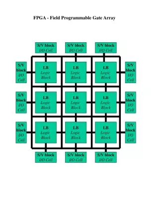
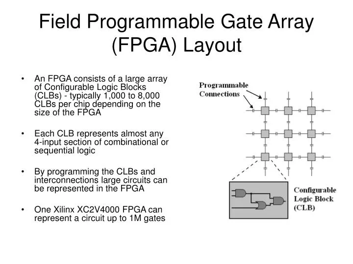
An FPGA consists of a large array of Configurable Logic Blocks (CLBs) - typically 1,000 to 8,000 CLBs per chip depending on the size of the FPGA Each CLB represents almost any 4-input section of combinational or sequential logic

E N D
An FPGA consists of a large array of Configurable Logic Blocks (CLBs) - typically 1,000 to 8,000 CLBs per chip depending on the size of the FPGA Each CLB represents almost any 4-input section of combinational or sequential logic By programming the CLBs and interconnections large circuits can be represented in the FPGA One Xilinx XC2V4000 FPGA can represent a circuit up to 1M gates Field Programmable Gate Array (FPGA) Layout
DINI DN3000k10 Board • DINI DN3000k10 is an FPGA based PCI card • Contains five Xilinx XC2V4000 FPGAs connected by a 226 bit wide bus • One of the FPGA has a separate connection for communicating to a PC via the PCI bus • FPGAs can be configured through the PCI bus or configurations can be stored on board
Multiplier Options Usage (% CLBs)* *Percentage of CLBs used in a XC2V4000, the XC2C4000 contains 5760 CLBs
Cellular Automata ModelMultiple Cells per Processing Element
Number of Processing Elements vs. Million Operations Per Second
Comparison to C-Simulation • Based on timing of optimized C simulation running on CCM1 (1.4GHz, 1GB RAM) • Simulator ran 1M iterations of a 5448 cell beam model in 111.4s - Million Cell Updates per Second: 48.9 • For a 5448 cell model at 16 bit precision the FPGA implementation could perform 7497M Cell Updates per Second • Based on these results the FPGA was ~150 times faster than the optimized C-simulation
Other FPGA Applications • HokieGene – Genome Matching Project (2003) • Matching engine executed on one FPGA (XC2V1000) • Performed 200 billion cell updates per second • 1,200 billion operations per second (1.2 GOPS) • BYU - Network Intrusion Detection Systems (2002) • Hardware implementation used one FPGA (XC2V1000) • Outperformed software version running on P3 – 750MHz: • Up to 400 times more throughput than software version • Up to 1000 times less latency than software version • Xilinx – High Performance DES Encryption (2000) • Implemented on one FPGA (XCV150) • Maximum throughput 10.75 GB/sec • Outperformed best ASIC implementation • Texas University – Target Recognition System (2000) • System built using one FPGA (ORCA 40k) and Myrinet interfacing • Capable of processing 900 templates per second • 2,800 billion operations per second (2.8 GOPS)