Download
1 / 20
200 likes | 269 Views
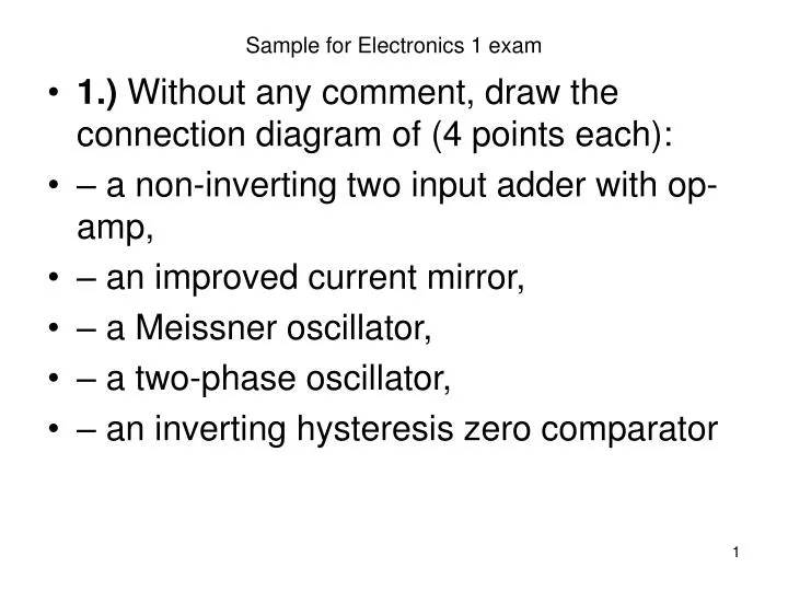
Sample for Electronics 1 exam. 1.) Without any comment, draw the connection diagram of (4 points each): – a non-inverting two input adder with op-amp, – an improved current mirror, – a Meissner oscillator, – a two-phase oscillator, – an inverting hysteresis zero comparator. v i1. v o.

E N D
Sample for Electronics 1 exam • 1.) Without any comment, draw the connection diagram of (4 points each): • – a non-inverting two input adder with op-amp, • – an improved current mirror, • – a Meissner oscillator, • – a two-phase oscillator, • – an inverting hysteresis zero comparator
vi1 vo vi2 Sample for Electronics 1 exam • – a non-inverting two input adder with op-amp
Iin Iout V+ Iin Iout Sample for Electronics 1 exam • – an improved current mirror • OR
1 : n VS+ L C vo VS- Sample for Electronics 1 exam • – a Meissner oscillator
vo1 vo2 Sample for Electronics 1 exam • a two-phase oscillator
Vref vo vi Sample for Electronics 1 exam • an inverting hysteresis zero comparator
Sample for Electronics 1 exam • 2.) Give the answer to the following questions in connection with feedback amplifiers: • a) What is the effect of a parallel current feedback on the transfer admittance, the transfer impedance, the input and output resistance of the amplifier (calculation formulas or qualitative statements, e.g. it will not be changed or it becomes smaller / larger etc.)? (8 points) • b) What do we call open-loop gain, closed-loop gain and loop gain (demonstrate the answers by the general block diagram of feedback)? (6 points) • c) When do we speak about 45 phase margin in case of an amplifier with feedback (illustrate it by a Nyquist or a Bode diagram)? (6 points)
S1 Si So + A - Sf=ßSo ß Sample for Electronics 1 exam • a.) • YA* = YA (does not change) • ZA*= ZA/(1+H) (decreases) • Rin*= Rin/(1+H) (decreases) • Ro*= Ro(1+ainHSp) (increases) • b.) • loop-gain H = Aß • open-loop gain A = So/S1 • closed-loop gain A* = So/Si
H, dB ImH =45 -20 dB/D -1 H0, dB 2 0 1 H (log) -40 dB/D Sample for Electronics 1 exam • C.) Nyquist Bode
Sample for Electronics 1 exam • 3.)a) Draw the principle connection of a complementary emitter-follower power amplifier. Give the condition for class B operation. Derive the calculation formulas for the supply power (PS), the output power (Pout) and plot their relative equivalents in a co-ordinate system as functions of the relative output amplitude. Designate in the so produced figure the total dissipated power (Pd). (14 points) • b) Draw the equivalent circuit for a SiO2 piezo-electric crystal, used in crystal oscillators, and give the diagram showing the absolute value of the impedance of the two-pole model as a function of the frequency, giving also the place and the calculation formulas of the series and parallel resonance frequencies. (6 points)
VS IC1 T1 vin io RL VB VB vo T2 IC2 -VS vin 1 PS rel t Pd rel IC1 2/ 0,5 I0 Pout rel 0 1 Sample for Electronics 1 exam • a.) • Condition for class B operation: VB = VBE th • the average of the current (I0): • I0 =2 v0p / RL 2π • Supply power: pS rel =(2/π)/(v0p/VS) • Output power: pout rel =0.5(v0p/VS)2
RS CS LS Z RS S P CP Sample for Electronics 1 exam • b.) • Equivalent circuit: • Frequency response: • ωs =1/sqrt(LsCs) • ωp =1/sqrt(Ls[CsxCp])
4R 3R ii R R vi A1 vo A2 4R R Sample for Electronics 1 exam • 4.)You are given the connection arrangement below. A1 and A2 are ideal op amps. • a) Determine the nominal voltage gain. (10 points) • b) Determine the input resistance. (10 points)
Sample for Electronics 1 exam • a.) Because A2 forms an inverting basic connection: Av2 = -3 • The inputs of A1 are equipotential, so: • … AvN =+3 • b.) … Rin = 2.5R
Sample for Electronics 1 exam • 5.)a) Draw the connection arrangement of a four bit weighted resistance D/A converter. (8 points) • b) The digital input code of an 8 bit D/A converter is D: 01010110, the reference voltage is Vref = 16 V and the applied code system is offset binary. Determine the value of the analog output voltage. (12 points)
MSB LSB Vref R R/23 R/2 R/22 I/23 I I/22 RF I/2 0 1 1 0 0 1 0 1 I V0 Sample for Electronics 1 exam • a.)
Sample for Electronics 1 exam • b.) • In the offset binary system: • V0 = VrefXD – 0.5Vref • …. V0 =-2.625
Sample for Electronics 1 exam • 6.)a) Draw the block diagram of a successive approximation A/D converter. (8 points) • The input voltage of a successive approximation A/D converter is: vin = 5,078125 V, the reference voltage is Vref = 10 V and the number of bits: n = 8. Determine the digital code at the end of the conversion process (D= ?). (12 points)
Vin comparator 1 2 controller and register clock D/A start n V0 ready display Sample for Electronics 1 exam • a.)
Sample for Electronics 1 exam • b.) • Step 1: V0 = 5 V (< 5.078125 V) → MSB (1st bit) = 1 • Step 2: V0 = 2,5 V (> 0.078125 V) → 2nd bit = 0 • Step 3: V0 = 1.25 V (> 0.078125 V) → 3rd bit = 0 • Step 4: V0 = 0.625 V (> 0.078125 V) → 4th bit = 0 • Step 5: V0 = 0.3125 (> 0.078125 V) → 5th bit = 0 • Step 6: V0 = 0.15625 V (> 0.078125 V) → 6th bit = 0 • Step 7: V0 = 0.078125 V (= 0.078125 V) → 7th bit = 1 and 8th bit =0. • Thus the solution: D: 10000010