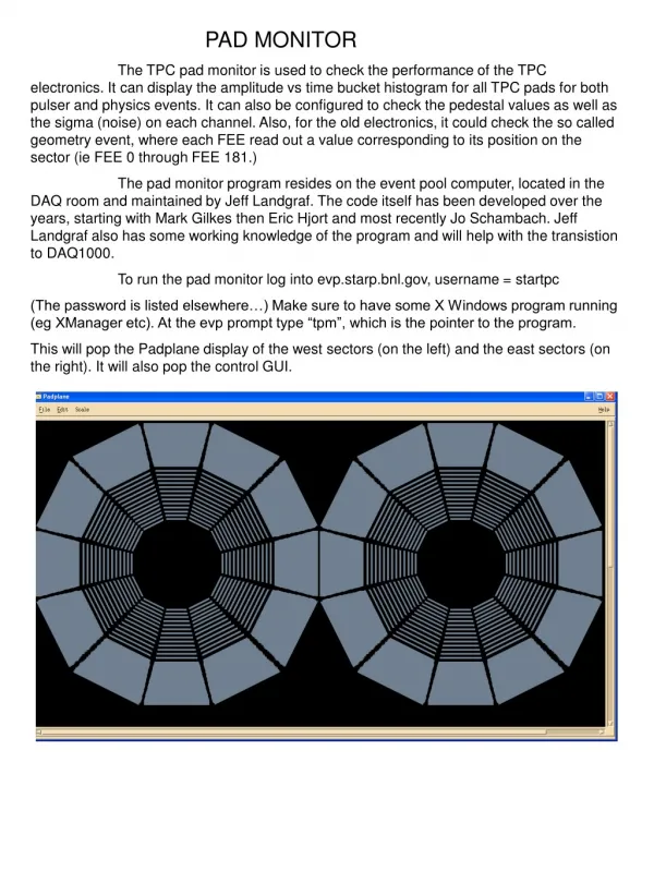
Download
1 / 19
190 likes | 322 Views
Digital Pad Operation. Christian Vega R . Jacob Baker UNLV Electrical & Computer Engineering . Digital I/O Pad. The pad also contains electrostatic discharge (ESD) diodes for protection from over voltages .

E N D
Digital Pad Operation Christian Vega R. Jacob Baker UNLV Electrical & Computer Engineering
Digital I/O Pad • The pad also contains electrostatic discharge (ESD) diodes for protection from over voltages • The digital I/O pad can be used for receiving data (input, sending data to circuitry on the chip) and transmitting data (output, sending data off chip) • D_Out is the connection for transmitting data out of the chip • En is the control connection; En = 1 puts the pad in transmitting mode, D_out is used while D_In and D_InB (complement of D_In) follow D_out and its complement respectively • En = 0 the pad is in the receive mode • En = 0 D_Out is a don’t care • D_In and D_InB are the true/complement inputs
Bidirectional Circuit The bidirectional circuit can be used to send signals off chip, to drive heavy loads, and for receiving signals, providing true and complement inputs The general schematic of the IO pad circuitry is seen below
Naming Convention For this tutorial we are using a the naming seen below
Naming Convention We will also divide the circuit into 8 stages to simplify the explanation shown below As a note for the following explanation VDD corresponds to logic 1 and ground or GND corresponds to logic 0
Driving A Signal On-Chip Let us set the enable (En) port to a logic 0 (ground), notice that in the first inverter stage MOSFET P1 is on and N1 is off so the value that passes through the node “oeb” is logic 1 due to that node being pulled up to VDD
Driving A Signal On-Chip Now for the second stage P2 is off and N2 is on so node “oe” is pulled down to ground (0)
Driving A Signal On-Chip Stages 3 and 4 get a little tricky to explain because the port D_out is introduced, so for the sake of the explanation we will set it to logic 1 With that P3 is turned off, P4 is turned off because its gate is tied to node “oeb” which is currently at 1 N3 is turned on because its gate is also tied to node “oeb”
Driving A Signal On-Chip For stage 4 the gates of P5 and N4 are tied to node “oe” which is set to 0 so P5 is turned on and N4 is turned off N5’s gate is tied to D_Out so it is set to 1 turning N5 on as a result, the nodes label “prep” is set to 1 and “pren” is set to 0 So due to this N6 and P6 are turned off
Driving A Signal On-Chip Now lets pause for a moment in order to evaluate the current operation the circuit is going under Setting the enable pin to 0 leads to stage 5 turning completely off (N6 and P6 are off) So the first 5 stages are cut off from the last two and the pad This is so a signal can be applied to the pin connected to the pad from the outside (so the pin is used as an input) If you noticed what you apply to D_Out does not matter because it will not pass through the 5th stage D_Out is used when you want to use the pad as an output to drive a load
Driving A Signal On-Chip With the previous in mind lets apply an arbitrary digital signal to the pad The signal will pass to the 6th stage which consists of an inverter that simply inverts the signal which goes to the port D_InB which is then supplied to the chip The now inverted signal is passed to stage 7 which is another inverter that supplies the original signal to the chip (port D_In)
Driving A Signal Off-Chip Lets now say that the chip generates a signal that needs to be sent out to drive a load, so lets set the enable (En) port to 1 In stage 1 P1 is shut off and N1 is turned on so node “oeb” is pulled down to 0
Driving A Signal Off-Chip So 0 passes to the next stage turning P2 on and N2 off Node “oe” is set to 1
Driving A Signal Off-Chip Now we are at the 3rd and 4th stage where D_Out is applied, lets say it is 1 P3 is turned off, while node “oeb” is at 0 so P4 is on and N3 is off
Driving A Signal Off-Chip For the next stage node “oe” as can be seen from earlier is currently at 1 so P4 is off while N4 is on The gate of N5 is tied to D_Out which is currently set to 1 so it is turned on
Driving A Signal Off-Chip For the 5th stage both nodes “prep” and “pren” are pulled down to 0 so P6 is on and N6 is off so what goes to the pad is 1 which is the value of D_Out The last two stages should not have an effect on this operation
Driving A Signal Off-Chip Lets take a moment to look at what happens if D_Out is set to 0 Nothing really changes except that P3 turns on and N5 turns off so the nodes “prep” and “pren” are pulled up to VDD (1) That value goes to the 6th stage and is inverted to a 0 which is the value of D_Out and that goes to the pad
Background Information Now that we have in detailed gone over the digital pad operation let us look at an actual layout of a digital pad on a real IC Layout with a close up of part of the bidirectional circuit
Background Information 40 pin quad frame layout