Download
1 / 6
70 likes | 193 Views
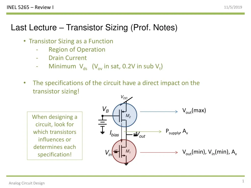
Last Lecture – Transistor Sizing (Prof. Notes). Transistor Sizing as a Function Region of Operation Drain Current Minimum V ds ( V ov in sat, 0.2V in sub V t ) The specifications of the circuit have a direct impact on the transistor sizing!. V DD. V B. V out (max). M 2.

E N D
Last Lecture – Transistor Sizing (Prof. Notes) • Transistor Sizing as a Function • Region of Operation • Drain Current • Minimum Vds (Vov in sat, 0.2V in sub Vt) • The specifications of the circuit have a direct impact on the transistor sizing! VDD VB Vout(max) M2 When designing a circuit, look for which transistors influences or determines each specification! Psupply, Av Ibias Vout Vout(min), Vin(min), Av Vin M1 Analog Circuit Design
Common Source Amplifier • where • VT0n=|VT0p|=1.0V • K’n=100µA/V2 • K’p=25µA/V2 • λn= λp =0.2V-1 • VDD=3.0V • Design the following CS amplifier for the following specifications: • Vout = [0.15 – 2.7] V • Psupply < 90μW • |Av| > 30 V/V VDD VDD M1 Vin Iref =10µA Vout M3 M2 Analog Circuit Design
Common Source Amplifier – with cascode • How the cascode transistor M2 affects the amplifier’s behavior? VDD VDD nMOS pMOS Vb M3 M1 Vin Vout Vcp M2 Vcn M2 Vout Vb Vin M1 M3 Analog Circuit Design
Common Source Amplifier – with cascode • Assuming Vto=0.7V and Vds(sat)=0.2V, for all transistor, find Vout(min) for all circuits. VDD VDD VDD Vb Vb Vb M3 M3 M3 Vout Vout Vout Vcn =1.1V Vcn =1V Vcn =1.4V M2 M2 M2 Vin Vin Vin M1 M1 M1 Analog Circuit Design
Asignación #1 • Fecha de entrega – lunes 14 de septiembre • Aprender a utilizar la herramienta CADENCE • Hacer el tutorial de cadence (~/public_cadence_1/gserrano/cadence_tutorial ) • Caracterización de Parámetros de los Transistores (L=1.8µm, W=6µm) • Extraer los parámetros en la región de saturación Kn’, Kp’, Vt0n, Vt0p, λn y λn utilizando las curvas apropiadas. • Entregar curvas utilizadas y el valor para cada uno de los parámetros (hacer énfasis en la región utilizada para extraer los parámetros) * Los modelos a utilizarse se encuentran en directorio ~/public_cadence_1/models * Utilizar los modelos ekv06P y ekv06N para simular la región de sub-Vt * Utilizar los modelos ami06P y ami06N para simular la región de saturación * Es posible utilizar Matlab para manejar la data (ver tutorial exporting_data_tutorial) Analog Circuit Design
Asignación #2 Fecha de entrega – viernes 29 de septiembre VDD Design the cascode current mirror for specifications provided. Simulate the proposed design and corroborate its performance. Iin Iout Ibias • Iout= 2·Iin=[0-10] µA • Vout(min) = 0.5V • Vin(max) = 0.9V + M3 M4 Vout • where • VT0n=|VT0p|=0.7V • K’n=100µA/V2 • K’p=25µA/V2 • λn= λp =0 M1 M2 _ Analog Circuit Design