Download
1 / 20
500 likes | 1.38k Views
Raman Spectroscopy of 2D Materials. Kevin Cai, AMSA Charter School Matthew Greenlaw , Pioneer Charter School of Science Dr. Birol Ozturk , Northeastern University Professor Swastik Kar , Physics, Northeastern University Laboratory for Graphene Research. 31 July 2014. Introduction.

E N D
Raman Spectroscopy of 2D Materials Kevin Cai, AMSA Charter School Matthew Greenlaw, Pioneer Charter School of Science Dr. BirolOzturk, Northeastern University Professor SwastikKar, Physics, Northeastern University Laboratory for Graphene Research 31 July 2014
Introduction • Graphene • 2D sheet of carbon • Conductor • Stronger than steel • Mechanical exfoliation, CVD • Applications • Films, composite materials • Biological engineering • Storage Image from http://en.wikipedia.org/wiki/Graphene
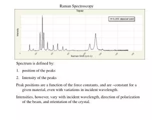
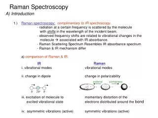
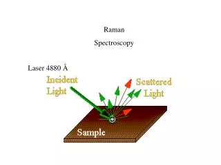
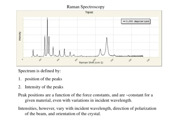
Raman Spectroscopy • Laser at set wavelength aimed at sample • Reflected beam has a different wavelength due to vibrations • Raman shift (wavenumber, cm-1)
Graphene’s Raman Spectrum • Three peaks • D peak (~1350 cm-1) – defect • G peak (~1600 cm-1) – in-plane vibrations • G’ peak (~2700 cm-1) – out-of-plane vibrations
Atomic Force Microscope (AFM) • Creates topographical image • Scanning probe (with laser aimed at the tip) vibrates at a set frequency/amplitude • Changes in amplitude are recorded
Objectives • How does the thickness of a graphene sample correlate to its Raman spectrum? • How does O2 flow rate affect the doping of graphene with boron nitride?
I - Mechanically Exfoliated Graphene • Procedure: • Exfoliate HOPG • Raman Spectroscopy • AFM • Graph IG’/IG ratio vs. thickness
Mechanically Exfoliated Graphene - Conclusions • IG’/IG ratio generally decreases as thickness increases • Along with lower intensity, G’ peak becomes wider with increasing thickness (multilayer)
II – BN-doped Graphene • Graphene – conductor, zero band gap • Boron nitride – semiconductor • Boron nitride domains are isostructuralto graphene • 2D semiconductor alloy with controlled band gap Image from: Servincli, H., et.al. “Effects of domains in phonon conduction through hybrid boron nitride and graphene sheets.” American Physical Society. 2011.
II – BN-doped Graphene • Procedure • Samples grown by CVD; B, N, C, and O present • O2 flow rates (sccm): 0, 2, 4, …, 10 • Raman Spectroscopy • Broad peak at ~1355 cm-1 decomposed • 1330 cm-1 (B-C peak), 1352 cm-1 (D peak), 1368 cm-1 (h-BN peak)
Conclusions • No clear trend found between O2 flow rate and h-BN domain coverage • More data needed
Future Work • Mechanically Exfoliated Graphene • Improve exfoliation strategy, scan/measure more samples • BN-doped Graphene • Use curve fitting on more Raman spectra of domains • Limit domain loss at higher O2 flow rate
References • [1] Servincli, H., et.al. “Effects of domains in phonon conduction through hybrid boron nitride and graphene sheets.” American Physical Society. 2011. <http://journals.aps.org/prb/abstract/10.1103/PhysRevB.84.205444>. • [2] Wang, Lifeng, et.al. “Monolayer Hexagonal Boron Nitride Films with Large Domain Size and Clean Interface for Enhancing the Mobility of Graphene- Based Field-Effect Transistors.”Wiley Online Library. 2014. <http://onlinelibrary.wiley.com/doi/10.1002/adma.201304937/full>. • [3] Zhou, H., Yu, F., Yang, H., Qiu, C., Chen, M., Hu, L., ... & Sun, L.. “Layer- dependent morphologies and charge transfer of Pd on n-layer graphenes”. Chem. Commun., 47(33), 9408-9410. (2011).
Acknowledgements • Dan Rubin and Dr. BirolOzturk – Research mentors • Center for STEM Education • Young Scholars Program and Team • Claire Duggan – Director • Kassi Stein, Jake Holstein, Chi Tse – Coordinators • Professor SwastikKar