Download
1 / 21
290 likes | 653 Views
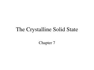
Contents. 1.8. The Crystalline State 1.9. Crystalline Defects and Their Significance 1.10. Single-crystal Czochralski Growth 1.11. Glasses and Amorphous Semiconductors 1.12. Solid Solutions and Two-Phase Solids 1.13. Bravais Lattices. 1. 8. The Crystalline State. c. . a. .

E N D
Contents 1.8. The Crystalline State 1.9. Crystalline Defects and Their Significance 1.10. Single-crystal Czochralski Growth 1.11. Glasses and Amorphous Semiconductors 1.12. Solid Solutions and Two-Phase Solids 1.13. Bravais Lattices
1. 8 The Crystalline State
c a b 1. 8 The Crystalline State Repetition of small cell of atoms unit cell See p.96 Infinite periodic arrays of geometric points in space, with no atoms
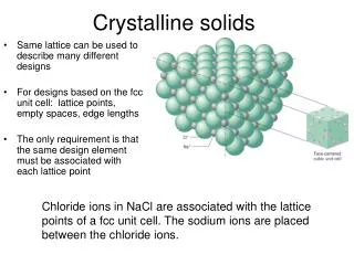
1. 8 The Crystalline State 1.8.1. Types of Crystals: characterized by unit cell, since the crystal is a periodic repetition of the unit cell • The Volume of the unit cell: 74% • Number of Atoms per unit Cell: 4 • ex) Cu, Ag, Al, Au, Ca, Ni See ex. 1.13 (p. 55) • The Volume of the unit cell: 68% • Number of Atoms per unit Cell: 2 • ex) Fe, Cr, Mo, W • The Volume of the unit cell: 74% • Number of Atoms per unit Cell: 2 • ex) Co, Mg, Ti, Zn
1. 8 The Crystalline State 1.8.1. Types of Crystals • Number of Atoms: 8 • ex) Diamond, Ge, Si • Number of Atoms: 4 cations + 4 anions • ex) LiF, MgO, CaO • Number of Atoms: 8 • ex) ZnS, GaAs, GaSb • Number of Atoms: 1cations + 1 anions (equal charges, same size) • ex) CsCl, CsBr
1. 8 The Crystalline State To discuss crystal structures, it is important to understand planes & directions in the lattice. (These 3 numbers define a set of parallel planes in the lattice)
1. 8 The Crystalline State
1. 8 The Crystalline State 1.8.2. Crystal Directions and Planes
1. 8 The Crystalline State A direction in a lattice is expressed as a set of 3 integers with the same relationship as the components of a vector in that direction.
1. 8 The Crystalline State 1.8.2. Crystal Directions and Planes
1. 9 Crystalline Defects and Their Significance There is no perfect crystal; so we must understand the type of defects in a given crystal structure. ‘M’ and ‘E’ properties may be controlled by these defects. 1.9.1. Point Defects: Vacancies and Impurities Point defect : due to lattice changes or distortions of a few atomic distances. • Substitutional impurity : The impurity atom substitutes directly for the host atom. • Interstitial impurity : The impurity atom can also place itself in an interstitial site. • Schottky defect : This involves a missing cation-anion pair which may have migrated to the surface • Frenkel defect : A host ion is displaced into an interstitial position, leaving a vacancy at its original site. examples
1. 9 Crystalline Defects and Their Significance 1.9.2. Line Defects: Edge and Screw Dislocations produced when an atomic plane terminates within the crystal instead of passing all the way to the end of the crystal. • edge dislocation : due to displacement of one plane to the other • screw dislocation : due to a shearing of one portion of the crystal with respect to another, by one atomic distance.
1. 9 Crystalline Defects and Their Significance 1.9.3. Planar Defects: Grain Boundaries • Because crystal orientation suddenly changes across the boundary, there are both voids at the grain boundary, and stretched and broken bonds planar defects • The grain boundary represents a high-energy region per atom with respect to the energy per atom within the bulk of the grains themselves. The atoms can diffuse more easily along a grain boundary because: ● Less bonds need to be broken due to the presence of voids. ● The bonds are strained and easily broken anyway. Solidification of a pc solid from the melt
1. 9 Crystalline Defects and Their Significance 1.9.4. Crystal Surfaces and Surface Properties. When the crystal lattice is abruptly terminated by a surface, <2D Si crystal lattice where each atom has 4 covalent bonds, each having 2 ‘e’> H on Si: chemical bond with a Si – chemisorption (ex. O2 on C) H2O on Si: secondary bond with a Si – physisorption (ex, Ni on Fe)
1. 9 Crystalline Defects and Their Significance 1.9.5. Stoichiometry, Nonstoichiometry, and Defect Structures. • Stoichiometric compounds are those that have an integer ratio of atoms. For example, as in CaF2 where two F atoms bond with one Ca atom.
1. 10 Single-Crystal Czochralski Growth Czochralski (CZ) crystal growth, the most common technique used for growing crystals for developing wafers, named in honor of its inventor, involves the crystalline solidification of atoms from a liquid phase at an interface. Procedures for CZ crystal growth: 1) A fused silica crucible is loaded with a charge of undoped EGS together with a precise amount of diluted silicon alloy. 2) The gases inside the growth chamber are then evacuated. 3) The growth chamber is then back-filled with an inert gas to inhibit the entrance of atmospheric gases into the melt during crystal growing. 4) The silicon charge inside the chamber is then melted (Si melting point = 1421 deg C). 5) A slim seed of crystal silicon (5 mm dia. and 100-300 mm long) with precise orientation tolerances is introduced into the molten silicon. 6) The seed crystal is then withdrawn at a very controlled rate. The seed crystal and the crucible are rotated in opposite directions while this withdrawal process occurs.
1. 11 Glasses and Amorphous Semiconductors 1.11.1. Glasses and Amorphous Solids • Crystal structure is characterized by its periodicity and degree of symmetry. But not all solids exhibit crystallinity. For example, SiO2 can be grown into crystalline or amorphous forms depending on the method of formation. • Many amorphous solids are formed by rapidly cooling or quenching the liquid to temperatures where the atomic motions are so sluggish that crystallization is virtually halted glasses <Crystalline and amorphous structures illustrated schematically in two dimensions>
1. 11 Glasses and Amorphous Semiconductors 1.11.2. Crystalline and Amorphous Silicon We can reduce the density of dangling bonds by terminating a dangling bond using H passivation Full covalent bond Each line = ‘e’ in a bond Broken bond Periodicity is lost
1. 12 Solid Solutions and Two-Phase Solids 1.12.1. Isomorphous Solid Solutions: Isomorphous Alloys solid solution (i.e., Cu-Ni alloy): - Isomorphous solid solution: The solid is a homogenous mixture of Cu and Ni atoms, with the same structure everywhere in the solid solution (a, b) • Interstitial solid solution: The solute atoms occupy interstitial sites, or voids between atoms in the crystal. (c) • Many solids are a homogeneous mixture of two types of separate atoms
1. 12 Solid Solutions and Two-Phase Solids 1.12.2. Phase Diagrams: Cu-Ni and Other Isomorphous Alloys Cooling behavior When a Cu-Ni alloy melts, melting temp. is not defined – S & L coexist In a homogenous chemical system - CuNi, one phase may be in contact with another phase
1. 13 7 Crystals and 14 Bravais Lattices All crystals can be classified into 7 crystals and 14 Bravais lattices – lattices whose unit cell is one of the 7 geometries shown in the figures below.