Download
1 / 66
660 likes | 684 Views
Computer Systems Unit 2 Computer Structure. Higher Grade Computing. Computer Organisation. Most computers still use the Von Neumann architecture. Computing problems are defined as a sequence of instructions ( program ) stored in main memory.

E N D
Computer Systems Unit 2 Computer Structure Higher Grade Computing
Computer Organisation • Most computers still use the Von Neumann architecture. • Computing problems are defined as a sequence of instructions (program) stored in main memory. • these are fetched in turn, decoded and executed by a processor.
Memory with program stored in it 10110100 10101101 01011011 10101001 01101010 ... Processor fetches, decodes and executes each program instruction
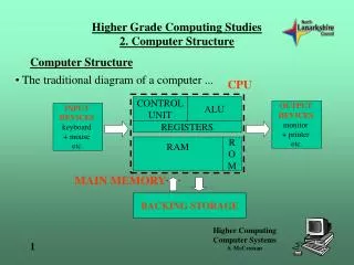
Structure of the CPU • Any program being executed is stored in the mainmemory of the computer. • Each program instruction (there may be millions) is fetched from memory, decoded then executed. • Each memory location has a unique address.
Block Diagram of a Computer Block Diagram of a Computer System Main Memory Input Processor Output Backing Storage = Data Flow B
The Structure of the Processor Main Memory Address Bus Other Registers MAR Data Bus MDR CU Control ‘Bus’ (read and write) ALU Clock Pulses Electronic Clock
The Processor • The processor contains: • the ALU • the registers • the control unit
The ALU • The ALU (Arithmetic Logic Unit) • carries out arithmetic operations such as add and subtract. • carries out logical operations such as ‘AND’ and ‘OR’.
The Control Unit • The control unit controls the fetching, decoding and executing of program instructions. • It is connected to the control‘bus’. • It sends and receives controlsignals to/from other parts of the computer.
The Registers • The registers are temporary storage locations inside the processor itself which can be accessed much faster than locations in main memory. • They are used for holding data, addresses or instructions.
Structure of the CPU • The CPU consists of the processor and memory. • The two are connected by three collections of wires called ‘buses’. • These are the address bus, the data bus and the control ‘bus’.
The CPU P r o c e s s o r M e m o r y Address bus Data bus Control ‘bus’
Address bus • The address bus carries signals from the processor to memory. • These signals specify which address in memory is to be read from or written to. • It is a one-way (‘uni-directional’) bus.
Address signal sent on address bus.. P r o c e s s o r M e m o r y Address bus ..’opens up’ specified memory location
Data bus • The data bus carries signals bothways between the processor and memory. • These signals are either program instructions or data. • The data bus is two-way (‘bi-directional’).
Control ‘bus’ • The control ‘bus’ is not a true bus. • It carries different lines each with their own separate functions. • Examples are: • read, write, clock, interrupt, reset
Control ‘bus’ lines • write • initiates a write to memory operation. • read • initiates a read from memory operation.
Control ‘bus’ lines • clock • carries signals from the clock chip which are used to synchronise events. • reset • clears processor registers and starts fetching from a pre-defined location.
Control ‘bus’ lines • IRQ (Interrupt Request) • carries signals from peripheral devices which require to be serviced. • NMI (Non-Maskable Interrupt) • carries urgent signals from peripherals which cannot be ignored.
Interrupts • An interrupt is a signal to the processor from an input or output device. • The interrupt system allows peripheral devices to communicate with the processor. • An interrupt: • Causes a break in the execution of the processors current program. • The processor saves a copy of what it is doing, runs a program to deal with the interrupt, then reloads its original task and continues. • A non-maskable interrupt behaves in the same way as an interrupt except that the processor cannot mask or ignore the interrupt.
Interrupts • Software can be used to make the processor ignore or mask the interrupt signal from a peripheral. • You would want to ensure that the processor ignored (masked) the fact that a printer had ran out of paper and not cause the processor to ‘hang’ waiting for paper to be added to the printer.
Read from memory P r o c e s s o r M e m o r y Address put on addressbus Data sent on data bus from specified memory address Read line on control ‘bus’ set
Write to memory P r o c e s s o r M e m o r y Address put on address bus Data sent on data bus to specified memory address Write line on control ‘bus’ set
Arithmetic Logic Unit Stack Pointer A B Instruction Register Control Unit Program Counter C D Memory Data Register Memory Address Register Address Bus Control ‘Bus’ Data Bus
Fetch Execute Cycle • Address of the next instruction to be fetched is transferred from the program counter and placed in the MAR and hence the address bus. Program Counter Memory Address Register Address Bus
Fetch Execute Cycle • The program counter is incremented to give the address of the next instruction in memory. 00001110 00001111 • The read line on the control bus is activated.
Memory Data Register Fetch Execute Cycle • The program instruction is read from the specified memory address and is transferred on the databus to the MDR. Instruction sent along data bus to MDR
Instruction Register Memory Data Register Fetch Execute Cycle • The program instruction is transferred from the MDR to the instruction register (IR) to be decoded and executed.
Read Operation from Memory • Processor sets up the address bus with the required memory address. It does this by placing a value in the MAR. • The Control Unit activates the READ line on the control bus. • The contents of the storage location in memory are released onto the data bus and placed into the MDR. • If this is an instruction it is decoded and executed.
Write Operation to Memory • Processor sets up the address bus with the required memory address. It does this by placing a value in the MAR. • The processor sets up the data bus with the value to be written to memory. It does this by placing the value in the MDR. • The Control Unit activates the WRITE line on the control bus. • The contents of the MDR are transferred to the storage location in memory.
Summary of the Fetch –Execute cycle • Processor sets up the address bus with the required address. • Processor activates the read line. • Instruction is transferred from memory to the processor by using the data bus (fetch). • The instruction is decoded. • The instruction is executed.
1 PC holds address of next instruction to be executed Fetch 0000 1111 1010 0100 6 (0110)
2. Put contents of PC into MAR Fetch 0000 1111 1010 0100 6 (0110) 6 (0110)
3. Read line is set (control bus) 1 Fetch 0000 1111 1010 0100 6 (0110) 6 (0110)
4. Clock pulse now causes Memory to place contents of that memory locationonto data bus 1 1 Fetch 0000 1111 1010 0100 1010 0100 6 (0110) 6 (0110)
5. Therefore that now appears in the MDR Fetch 0000 1111 1010 0100 6 (0110) 6 (0110) 1010 0100
6. This is a program instruction, so this is now placed into the IR Fetch 0000 1111 1010 0100 6 (0110) 1010 0100 6 (0110) 1010 0100 It is known that this is a program instruction as this came originally from the PC
7. The PC is now incremented Fetch 0000 1111 1010 0100 7 (0111) 1010 0100 6 (0110) 1010 0100
Memory/Storage • There are four main types of computer storage: • backing storage (largest) • main memory • cache memory • registers (smallest)
1 Backing storage • Backing storage is where programs and data are stored permanently until required. • Backing storage allows backup copies of data to be kept. • Examples are hard drives, CD-R, CD-R etc.
2 Main Memory • Main memory is where: • programs are held while being run. • data created by programs or entered by the user is stored . • Main memory consists of: • ROM and RAM.
2 Main Memory • ROM (Read Only Memory) • holds system programs needed at start up (e.g. bootstrap loader). • contents are permanent. • user cannot change contents of ROM.
2 Main Memory • RAM (Random Access Memory) • Holds programs and data loaded in from backing storage. • Holds data typed in by user. • User can change contents of RAM. • Contents disappear at power off. • DRAM and SRAM. • Dynamic – has to have its data consistently refreshed or it is lost. • Static – does not need to have its contents constantly refreshed.
3 Cache memory • Special very fast access memory between the rest of the main memory and the processor. • Frequently used program instructions and data are copied there to speed up processing. • There are usually 2 levels of Cache memory: • Level 1 – usually built into the processor chip (ultra close to the ‘action’). • Level 2 – may be on the chip as well but more often very close to it. • It is much faster for the processor to access data held in Cache than in main memory.
3 Cache memory very fast access fast access Processor Cache memory Main memory
4 Registers • Registers are fast access temporary storage within the processor which can hold: • data (MDR). • an instruction being executed (the instruction register (IR)). • the address to be accessed (MAR).
Arithmetic Logic Unit Stack Pointer A B Instruction Register Control Unit Program Counter C D Memory Data Register Memory Address Register Address Bus Control ‘Bus’ Data Bus
Summary of memory/ storage • In ascending order of speed of access: • Backing storage (slowest) • Main memory • Cache memory • Internal processor registers (fastest)
Addressability of memory • The place where each item is stored in a computers memory is important because the computer has to be able to find any given item of data. • An item is stored in memory in a storage location. • Each location in main memory is identified by a unique binary number called its address. The method a computer uses to identify storage locations is called its addressability. • Addresses start at zero and go up to a number which is determined by the width of the address bus.
E.g. with an 8-bit address bus: Address Contents 00000000 10101101 00000001 11010111 00000010 00110101 00000011 10101001 …. …. 11111111 01101010