Download
1 / 25
250 likes | 353 Views
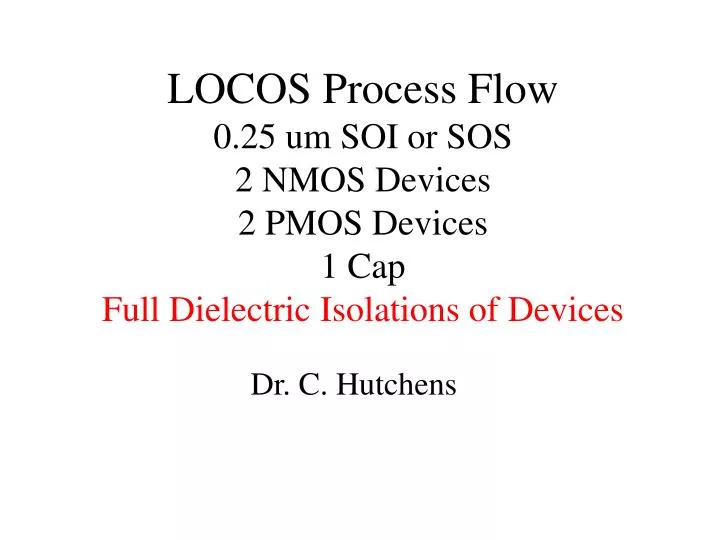
LOCOS Process Flow 0.25 um SOI or SOS 2 NMOS Devices 2 PMOS Devices 1 Cap Full Dielectric Isolations of Devices. Dr. C. Hutchens. Device Symbol plus Parasitics. The Device The Magic. Tenth Year SOI taught at OK STATE Now used by – Most IC manufactures except Intel. Recent AMD production.

E N D
LOCOS Process Flow0.25 um SOI or SOS2 NMOS Devices2 PMOS Devices1 CapFull Dielectric Isolations of Devices Dr. C. Hutchens
Device Symbolplus Parasitics The Device The Magic Tenth Year SOI taught at OK STATE Now used by – Most IC manufactures except Intel. Recent AMD production Parasitics
Starting SOI Material 200 to 300 mm Dia. Wafer 900 + Athalons/Wafer x 100+ Wafers/run …. 3 runs/day = 270,000 chips 10 Weeks (70 days) to completions 19 Million chips or $1 Billion Silicon (~450 Å = 45nm) SiO2 (BOX, ~1450Å) P-substrate Si (~650 um)
Stress-Relief Oxidation ~50 Å Silicon (~450 Å) SiO2 (BOX, ~1450 Å) P-substrate
Initial Implant –”Establish known baseline” Set nominal n or p Substrate doping level. ~50 Å Silicon (~450 Å) SiO2 (BOX, ~1450 Å) P-substrate
Nitride Deposition Silicon Nitride (~1200 Å) ~50 Å Silicon (~450 Å) SiO2 (BOX, ~1450 Å) P-substrate
Nitride/ SiO2 /Si Etch (ISL mask) NOTE: Nitride protects the Si island region from oxidizing in the next oxidation step (FOX) Si Island to be Multiple Islands for Transistors and Caps photoresist photoresist Silicon Nitride Silicon Nitride Si Silicon (~45 nm) Si SiO2 (BOX, ~1450 Å) P-substrate
LOCOS Oxidation Note increased height of FOX Si + H2O+ Heat = SiO2 SiO2 (~2.2x45 nm) Si: SiO2 = 0.45 Ratio Nitride FOX (~3K Å ) FOX (~115 Å ) Si SiO2 (BOX, ~1450 Å) P-substrate
Etch Nitride + Stress Relief Oxide FOX (~99 Å ) Si SiO2 (BOX, ~1450 Å) P-substrate
Initial Oxide Deposition Capacitor function #gate oxide growth – Dry O2 + heat Thermal Oxide diffus time=99? temp=825 dryo2 press=1.00 hcl=0diffus time=10 temp=825 nitro press=1.00 hcl=0 ~100 Å Si SiO2 (BOX, ~1450 Å) P-substrate
Cap Implant (DF mask ?) Depletion mode N MOSFET S/D Implants G S/D Photo resist blocks doping when energy level is set appropriately. S/D S/D Gate to be photoresist ~100 Å Si SiO2 (BOX, ~1450 Å) P-substrate
PWELL Implants -2X (NMOS Threshold voltage Nominal and High) #Screening oxide 50 A deposit oxide thick=0.005 divisions=3 # Channel Doping for NFET implant boron dose=6e12 energy=8 tilt=7 rotation=0nominal N ~50 Å photoresist photoresist photoresist photoresist FOX FOX FOX FOX Si Si Si Si Si Si Si SiO2 (BOX, ~4000 Å) SiO2 (BOX, ~1450 Å) P-substrate
NWELL Implants – 2X (PMOS Threshold voltage Nominal and High) #Screening oxide (not a thermal oxide) 50 A deposit oxide thick=0.005 divisions=3 # Channel Doping for PFETimplant phosphor dose=6e12 energy=40 tilt=7 rotation=0nominal P photoresist photoresist photoresist photoresist FOX FOX FOX FOX Si Si Si Si Si Si Si SiO2 (BOX, ~4000 Å) SiO2 (BOX, ~1450 Å) P-substrate
Gate Oxidation – TOX in Cgs • Remove screening Oxide • Grow thermal gate Oxide #5nm gate oxide grown diffus time=27 temp=825 dryo2 press=1.00 hcl=0 diffus time=10 temp=825 nitro press=1.00 hcl=0 TOX ~50 Å Si Birds Beak effect C overlap Birds Beak effect C overlap SiO2 (BOX, ~4000 Å) SiO2 (BOX, ~1450 Å) P-substrate
Poly Deposition and Implant n-ploy Set Gate work function – Threshold Voltage implant phosphor dose=15.0e15 energy=40 pearsondiffus time=5 temp=825 nitro press=1.00implant phosphor dose=15.0e15 energy=20 pearsondiffus time=2 temp=750 nitro press=1.00 POL( ~1600 Å) ~50 Å Si SiO2 (BOX, ~145 Å) P-substrate
Poly Deposition and Implant p-ploy Set Gate work function – Threshold Voltage implant bf2 dose=10.0e15 energy=45 pearsondiffus time=5 temp=750 nitro press=1.00implant bf2 dose=10.0e15 energy=25 pearsondiffus time=2 temp=750 nitro press=1.00implant bf2 dose=10.0e15 energy=15 pearson POL( ~1600 Å) ~50 Å Si SiO2 (BOX, ~145 Å) P-substrate
Poly Etch and MDD IMPLANT – typical of 4 1) Set Gate geometry; “L, the 0.25um this process” 2) Reduce punch through implant arsenic dose=4.0e13 energy=15 tilt=45 rotation=0 amorph \ lat.ratio1=1.0 lat.ratio2=1.0 implant arsenic dose=4.0e13 energy=15 tilt=45 rotation=90 amorph \ lat.ratio1=1.0 lat.ratio2=1.0 implant arsenic dose=4.0e13 energy=15 tilt=45 rotation=180 amorph \ lat.ratio1=1.0 lat.ratio2=1.0 implant arsenic dose=4.0e13 energy=15 tilt=45 rotation=270 amorph \ lat.ratio1=1.0 lat.ratio2=1.0 Drain Source Gate POL( ~1600 Å) ~50 Å Si ++++ + + + + ++++ SiO2 (BOX, ~145 Å) SiO2 (BOX, ~4000 Å) P-substrate
Oxide 850 A – typical of 4 Spacer adds to CGDO of model # Deposit Spacer Oxide 850 A rate.depo machine=PECVD oxide a.m cvd dep.rate=100 step.cov=0.60 deposit machine=PECVD time=8.5 #Etch Spacer Oxide, 1050 A and TOX 50A etch oxide dry thick=0.090 #etch silicon dry thick=.015 Drain Gate Source POL( ~1600 Å) ~50 Å Si ++++ + + + + ++++ SiO2 (BOX, ~145 Å) SiO2 (BOX, ~4000 Å) Adds to RD/RS and CGDO Adds to RD/RS and CGDO P-substrate
Spacer Oxide 850 A Overlap Cap and birds beak Gate Gate POL( ~1600 Å) ~50 Å Si SiO2 (BOX, ~4000 Å) SiO2 (BOX, ~1450 Å) P-substrate
Cobalt Silicidation of Silicon D/S and Gate Decrease Resistance S/D and Gate to 4-6 ohms/sq deposit cobalt thick=16 nm divisions=3 diffus time=3.5 temp=550 nitro press=1.00 Gate Gate POL( ~1600 Å) ~50 Å Si SiO2 (BOX, ~4000 Å) SiO2 (BOX, ~1450 Å) P-substrate
Process Simulation – Normal NMOS - “PD” Gate CoSi Gate poly Oxide Spacer TOX Al S/D CoSi Diode Junction Device Channel Si Island BOX Substrate This is the ONLY properly scaled diagram in the presentation.
Process Simulation – Normal NMOS - “PD” VT = 0.45 ID (VDD=3.3V) = 1.4mA/um NGate - 6E18/cm3 PChannel - 1E17/cm3 NLDD - 3E18/cm3 Lov -13nm (Lov >2-3Tox)1 RLDD -5000 ohms/sq Note1-Chan et. al.
Process Simulation – HVT NMOS - FD VHTN = 0.95 ID (VDD=3.3V) = 1.1mA/um VNTN = 0.45 ID (VDD=3.3V) = 1.4mA/um PGate - 2E19/cm3 PChannel - 2E15/cm3 NLDD - 8E17/cm3 Lov -20nm (Lov >2-3Tox) RLDD -10k ohms/sq
Process Simulation – Normal PMOS - “PD” VT = -0.42 ID (VDD=-3.3V) = 0.51mA/um VGS = 0.5,1.1,2.2,3.3 PGate - 3E19/cm3 NChannel - 5E17/cm3 PLDD - 3E18/cm3 Lov -12nm (Lov >2-3Tox) RLDD -10K ohms/sq
Process Simulation – HVT PMOS - FD VHTN = 0.96 ID (VDD=-3.3V) = 0.44mA/um NGate - 2E20/cm3 NChannel - 2E16/cm3 PLDD - 8E17/cm3 Lov -20nm (Lov >2-3Tox) RLDD -20k ohms/sq