Download
1 / 42
460 likes | 696 Views
Chapter 7 EGR 270 – Fundamentals of Computer Engineering. 1. Reading Assignment: Chapter 7 in Logic and Computer Design Fundamentals, 4 th Edition by Mano. Chapter 7 – Counters and Registers

E N D
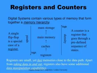
Chapter 7 EGR 270 – Fundamentals of Computer Engineering 1 Reading Assignment: Chapter 7 in Logic and Computer Design Fundamentals, 4th Edition by Mano • Chapter 7 – Counters and Registers • In chapter 6 we explored methods of designing synchronous sequential circuits. Chapter 7 introduces asynchronous sequential circuits (ripple counters) as well as registers and other examples of counters. • Counters • Two types of counters are commonly available: • 1) synchronous counters • a) all flip-flops clock inputs are tied together so that the flip-flops are clocked synchronously • b) counters can be designed using standard synchronous sequential circuit design methods (such as the excitation table method, the state equation method, and the “one-hot” method) • 2) asynchronous counters (ripple counters) • a) not all flip-flops are clocked synchronously - clock inputs may come from • various points • b) standard synchronous sequential circuit design methods cannot be used (we have no clear methods, but we will study some existing designs to see how they work).
Chapter 7 EGR 270 – Fundamentals of Computer Engineering 2 Q1 (LSB) Q2 Q3 (MSB) J1 Q1 J2 J3 Q3 1 1 1 Q2 Clock K3 1 K1 1 K2 1 Q1 Q2 Q3 Clock Q1 Q2 Q3 Count 0 Ripple Counters Example 1: Draw a timing diagram for the 4-bit ripple counter shown below in order to determine its counting sequence. Discuss why this is a ripple counter and not a synchronous counter. Begin with count 0.
Chapter 7 EGR 270 – Fundamentals of Computer Engineering 3 Q1 (LSB) Q2 Q3 (MSB) Q1 J2 Q2 1 1 1 J3 Q3 J1 Clock K2 Q2 1 1 1 K3 Q3 Q1 K1 Clock Q1 Q2 Q3 Count 0 Ripple Counters Example 2: Repeat Example 1 using positive-edge triggered flip-flops.
Chapter 7 EGR 270 – Fundamentals of Computer Engineering 4 Q1 (LSB) Q2 Q3 (MSB) Q1 J3 J1 J2 Q2 Q3 1 1 1 Clock K1 K2 K3 1 Q1 1 Q2 1 Q3 Clock Q1 Q2 Q3 Count 0 Ripple Counters Example 3: Repeat Example 1 with clock for flip-flopN= Q’N-1for N > 1.
Chapter 7 EGR 270 – Fundamentals of Computer Engineering 5 Q1 (LSB) Q2 Q3 (MSB) 1 1 J2 1 Q3 Q2 J3 J1 Q1 Clock 1 1 1 K2 K1 K3 Q1 Q2 Q3 Clock Q1 Q2 Q3 Count 0 Ripple Counters Example 4: Repeat Example 3 with positive-edge triggered flip-flops.
Chapter 7 EGR 270 – Fundamentals of Computer Engineering 6 Summary Notes: 1) The type of triggering is often irrelevant with synchronous counters. All of our examples in Chapter 6 (and in lab) could have used any type of triggering. 2) The type of triggering used in ripple counters is important and may affect circuit operation. 3) All flip-flops are clocked by the same source (i.e., synchronously) in synchronous circuits. 4) All flip-flops are not clock by the same source in asynchronous (ripple) counters. The choice of the clocking signal for each flip-flop is critical.
Chapter 7 EGR 270 – Fundamentals of Computer Engineering 7 Q1 (LSB) Q2 Q3 (MSB) J2 1 1 1 J1 Q1 Q2 J3 Q3 Clock 1 1 1 K1 Q1 K2 K3 Q3 Q2 Clock Q1 Q2 Q3 Count 0 Propagation Delay- Propagation delay can be a problem in ripple counters at high frequency as the clock signals “ripple” though the circuit. Example 5: Repeat example 1 using an input 10 MHz clock and a propagation delay of 20 ns.
Chapter 7 EGR 270 – Fundamentals of Computer Engineering 8 PSPICE Example: 3-Bit Ripple Counter(see Bb or course website). Note that this circuit matches the previous example, including the 10MHz clock.
Chapter 7 EGR 270 – Fundamentals of Computer Engineering 9 • Commercially-available Counters • Both synchronous and asynchronous (ripple) counters are available commercially. • 7490 Decade Counter – synchronous counter or ripple counter? • 74190 Up/Down Decade Counter - synchronous counter or ripple counter?
Chapter 7 EGR 270 – Fundamentals of Computer Engineering 10 Q1 (LSB) Q2 Q3 Q4 (MSB) J2 J4 Q1 J3 1 J1 Q2 1 Q3 Q4 Clock K4 K2 K3 1 1 1 1 K1 Q1 Q2 Q3 Q4 Clock J2 K2 J4 K4 C Q1 Q2 Q3 Q4 Count 0 Example 6: Use a timing diagram to determine the counting sequence for the ripple counter below. Begin with count 0.
Chapter 7 EGR 270 – Fundamentals of Computer Engineering 11 • Synchronous Counters • Synchronous counters have all flip-flop clock inputs tied together and clocked simultaneously. • Synchronous counter may be designed by: • The excitation table method (covered earlier) • The state equation method (covered earlier) • The “one-hot” method (covered earlier) • By inspection (for relatively simple counters) – covered below • Synchronous Counter Design by Inspection • This method is sometimes useful for simple counter designs. • This method may not yield the simplest solution, but it is typically easy to perform. • Based on the use of T flip-flops (or JK flip-flops in the toggle mode). Determine when each flip-flop must toggle by observing the bit changes in the counting sequence.
Chapter 7 EGR 270 – Fundamentals of Computer Engineering 12 Example: Design a 4-bit synchronous counter using the inspection method and JK flip-flops.
Chapter 7 EGR 270 – Fundamentals of Computer Engineering 13 • N-bit synchronous counter • Show how an n-bit counter can be implemented using N flip-flops and (N-2) two-input AND gates • Discuss the delay problems • Show how the delay can be improved by using ANDs with increasing numbers of inputs
Chapter 7 EGR 270 – Fundamentals of Computer Engineering 14 Example: Design a 5-bit synchronous up/down counter using the inspection method and JK flip-flops. Discuss the amount of work involved in a similar design using the excitation table method.
Chapter 7 EGR 270 – Fundamentals of Computer Engineering 15 • Timing Sequences • So far we have designed circuits to: • produce desired outputs for certain input combinations (combinational circuits) • produce a desired sequence of states or input output sequence (sequential circuits) • One type of circuit that we have not directly dealt with is a circuit that will produce a series of control signals (or timing sequences) where each signal is HIGH or LOW for a specified length of time. • Such timing sequences are often needed. Examples might include: • signals to stop, start, and control the length of time for each cycle in a washing machine • signals to control the RED, YELLOW, and GREEN signals for a stop light • signals to control the opening and closing of valves
Chapter 7 EGR 270 – Fundamentals of Computer Engineering 16 Decoders – Can be used to indicate when certain counts occur. Similarly, they can be used to start or stop events at certain times. Example: Design a decoder to detect when count 4 occurs in a 3-bit counter. (Use an AND gate and inverters) Example: Design a decoder to detect when counts 1, 5, or 7 occur in a 3-bit counter. (Use a 3x8 decoder and an OR gate.)
Chapter 7 EGR 270 – Fundamentals of Computer Engineering 17 Example: Design a circuit that will output a signal that is HIGH for 3 seconds and LOW for 5 seconds.
Chapter 7 EGR 270 – Fundamentals of Computer Engineering 18 Example: Design a circuit that will produce the following control signals.
Chapter 7 EGR 270 – Fundamentals of Computer Engineering 19 Example: Design a traffic light controller with the following control signals. Notes: Whenever N/S Green or N/S Yellow are HIGH, E/W Red must also be HIGH. Whenever E/W Green or E/W Yellow are HIGH, N/S Red must also be HIGH. (Discuss the design then view the circuit simulated in PSPICE on the following slides.)
Chapter 7 EGR 270 – Fundamentals of Computer Engineering 20 Example:Traffic light controller (continued)
Chapter 7 EGR 270 – Fundamentals of Computer Engineering 21 Example:Traffic light controller (continued)
Chapter 7 EGR 270 – Fundamentals of Computer Engineering 22 Example:Traffic light controller (continued)
Chapter 7 EGR 270 – Fundamentals of Computer Engineering 23 • Shift Registers • Register - a group of binary storage cells (flip-flops) • Common Register Uses: • Temporary data storage and transfer • Parallel-to-serial and serial-to-parallel conversion • Data manipulation (complementation, rotation, etc) • Shift register - A register is often also referred to as a "shift register" since one of its key functions involves the shifting of data through the register. Example: A register might be a group of 8 flip-flops used to store some binary data (byte or word). Sketch the circuit.
Chapter 7 EGR 270 – Fundamentals of Computer Engineering 24 Common register functions: (briefly illustrate each) 1) Serial shifting of data (SISO - right or SISO - left) (SISO = Serial-input, Serial-output) 2) Parallel input of data (PI) 3) Parallel output of data (PO) 4) Rotation of data (left or right)
Chapter 7 EGR 270 – Fundamentals of Computer Engineering 25 Example: Discuss the registers in the 68HC11 and some specific register instructions.
Chapter 7 EGR 270 – Fundamentals of Computer Engineering 26 Parallel load shift register using D flip-flops– illustrate
Chapter 7 EGR 270 – Fundamentals of Computer Engineering 27 Parallel load shift register with an enable Discuss the limitations of the prior shift register (loads on every clock pulse). Show how to implement the register above using SR or JK flip-flops and then add an Enable line (ANDed with each input).
Chapter 7 EGR 270 – Fundamentals of Computer Engineering 28 Serial-In Serial-Out (SISO) register Illustrate using D flip-flops and JK flip-flops.
Chapter 7 EGR 270 – Fundamentals of Computer Engineering 29 Rotation of data Illustrate rotate-right and rotate-left registers using D flip-flops and JK flip-flops.
Chapter 7 EGR 270 – Fundamentals of Computer Engineering 30 Multi-function shift register Design a shift register with two mode controls, x and y, that will function as follows (fill in the input connections for D0 – D3). Draw the shift register. Show how to use either logic gates or multiplexers for the input connections.
Chapter 7 EGR 270 – Fundamentals of Computer Engineering 31 7495 Data Sheet. Discuss the features available on this 4-bit shift register.
Chapter 7 EGR 270 – Fundamentals of Computer Engineering 32 Input A Output Y = A if C = 1 High Z if C = 0 Control C Tri-state buffer Reading Assignment:Sections 2.10 and 7.8 in Logic and Computer Design Fundamentals, 4th Edition by Mano • Three-State Devices (Tri-State Devices) • Devices used so far have two output states: logic 0 or logic 1 • Tri-state devices have three output states: • Logic 0 • Logic 1 • High impedance (Z) state • When a tri-state device is in the high Z state, the output appears to be disconnected. This allows several outputs to be connected together, such as in the case where several outputs are connected to a common bus. • Although tri-state outputs are available with various types of gates, the most common is probably the tri-state buffer.
Chapter 7 EGR 270 – Fundamentals of Computer Engineering 33
Chapter 7 EGR 270 – Fundamentals of Computer Engineering 34 Octal 3-state buffer: Reference: John Wakerly, Digital Design – Principles & Practices, 3rd Edition, Prentice-Hall
Chapter 7 EGR 270 – Fundamentals of Computer Engineering 35 1 0 0 1 4-bit bus 0 1 1 0 Z Z Z Z Z Z Z Z 0 1 0 0 1 0 1 0 1 0 1 1 1 0 0 Bus Controller Device 1 Device 2 Device 3 Application: Connecting several peripheral devices to a bus Can be used to indicate when certain counts occur. Similarly, they can be used to start or stop events at certain times. Note in the example below that the bus controller connects Device 2 to the bus and Devices 1 and 3 are in the high-Z state.
Chapter 7 EGR 270 – Fundamentals of Computer Engineering 36 Rather than show each wire in a bus, it is more convenient to show a bus as follows: 8 Notation for an 8-bit bus The last diagram repeated using bus notation: 4 1 Z Z 4 4 4 1 0 0 Bus Controller Device 1 Device 2 Device 3
Chapter 7 EGR 270 – Fundamentals of Computer Engineering 37 Application: Using two 74541 IC’s to connect two 8-bit user inputs to a common data bus (DB) connected to a microprocessor Reference: John Wakerly, Digital Design – Principles & Practices, 3rd Edition, Prentice-Hall
Chapter 7 EGR 270 – Fundamentals of Computer Engineering 38 Transceiver - A device capable of transferring information in either direction. A transceiver can be constructed using two tri-state buffers along with some control logic, as shown below. A B Enable Direction Enable 0: enable transceiver 1: disable transceiver Direction 0: transfer A to B 1: transfer B to A Buffer Control Lines 1: enable buffer 0: disable buffer (high Z)
Chapter 7 EGR 270 – Fundamentals of Computer Engineering 39 A A A B B B Enable Enable Enable Direction Direction Direction Illustration – Add logic values to the diagrams below to illustrate the transceiver operation. Case 1: Enable = 1 Case 2: Enable = 0 Direction = 0 Case 3: Enable = 0 Direction = 1
Chapter 7 EGR 270 – Fundamentals of Computer Engineering 40 Octal 3-state transceiver: Reference: John Wakerly, Digital Design – Principles & Practices, 3rd Edition, Prentice-Hall
Chapter 7 EGR 270 – Fundamentals of Computer Engineering 41 Figure 5-60 Bidirectional buses and transceiver operation. Application: Octal 3-state transceiver used to connect two data buses: Reference: John Wakerly, Digital Design – Principles & Practices, 3rd Edition, Prentice-Hall
Chapter 7 EGR 270 – Fundamentals of Computer Engineering 42 Tri-state outputs with PLD’s: Recall that the GAL22V10 PLD was discussed earlier. It has 22 Output Logic MacroCells (OLMCs) that can be configured as inputs or outputs. How is this possible? By using tri-state buffers.