Download
1 / 38
380 likes | 479 Views
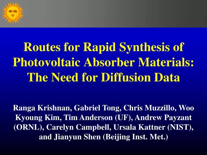
Routes for Rapid Synthesis of Photovoltaic Absorber Materials: The Need for Diffusion Data. Ranga Krishnan, Gabriel Tong, Chris Muzzillo , Woo Kyoung Kim, Tim Anderson (UF), Andrew Payzant (ORNL), Carelyn Campbell, Ursala Kattner (NIST), and Jianyun Shen ( Beijing Inst. Met.).

E N D
Routes for Rapid Synthesis of Photovoltaic Absorber Materials: The Need for Diffusion Data Ranga Krishnan, Gabriel Tong, Chris Muzzillo, Woo Kyoung Kim, Tim Anderson (UF), Andrew Payzant (ORNL), Carelyn Campbell, UrsalaKattner (NIST), and JianyunShen(Beijing Inst. Met.)
Jevons Paradox Technological progress that increases the efficiency with which a resource is used, tends to increase (rather than decrease) the rate of consumption of that resource. William Stanley Jevons
Simple Diode Analysis for a 24%-efficient Si solar cell Energy (eV) Unused Photons 19% Maximum energy collected = Egap 31% Loss for Energy above Egap Intensity (mW/m2-mm) Other losses: Absorption Collection Reflection Series R Shunts Voc < Egap 16% Fill Factor 5% Other Losses 5% Photons used Usable power 24% Wavelength (nm)
Photovoltaic Technologies First generation Single crystal and multicrystalline Si a-Si:H single junctions Second generation Inorganic thin films (CuInSe2 & CdTe) Multijunction III-V & a-Si:H Third generation Nanostructured & quantum dot PV Photoelectrochemical cells Organic photovoltaics Intermediate band concepts United solar Shell Solar Solarmer OPV module (PV-Tech.org) CdTe nanorods N. Lewis, Caltech
Ni/Al grid AR coating ZnO n-CdS p-CIGS absorber c Cu Sputtered Mo In or Ga Se Substrate a Chalcopyrite structure a CIGS solar cell structure Cu(In1-xGax)Se2Solar Cells Most Promising Thin Film Absorber Material • Direct band gap (Eg ~ 1.2 eV) • High optical absorption coefficient: ~ 2 m • High radiation resistance • High reliability • Lower cost per Watt installed • High conversion efficiency: cell: 20% and module: 13% • Efficient in low-angle & low-light conditions • Flexible substrates possible (BIPV, cheaper substrates?) • Positive response under concentration
1st stage 2nd stage 3rd stage 600 C 12 Open shutter 10 400 C 8 Se 30 6 In Metals rates (Å/s) 20 Cu 4 Se rate (Å/s) Ga In 10 2 Ga 0 0 -10 0 10 20 30 40 50 60 Run time (min) NREL 3-stage Process: Champion Cell
Module costs must be considered in the context of module efficiency (impact on installation costs) CIGS Manufacturing Costs Courtesy of NREL
The Value Proposition for High Efficiency CIGS Courtesy of NREL • At no added cost ($/m2), 17.5% CIGS module = ~$0.50/Wp module ASP target • New champion lab cell efficiency (≥22%), BoS improvements are required
ZnO, ITO (2500 Å) • Sputter • CdS (700 Å) • Chemical Bath Deposition • Sputter • CIGS (1-2.5 µm) • Multiple methods(coevaporation,sputtering,printing,electrodeposition) • Mo (0.5-1 µm) • Sputter Glass,Metal Foil,Plastics Future Challenges and OpportunitiesDevice structure varies between monolithically & mechanically integrated modules Forward Today Front Contact Grid • Reduce shadowing • Faster application • Screen Print Ag Hardened TCO (moisture barrier) Cd-free; dry, eliminate Increase Ga-%, Reduce thickness, Rapid deposition Uniformity (composition, temp., thickness) Na dosing High temp. glass Metal foils: smooth, flex-dielectric (monolith.)
Seek CIGS Pathway High-rate High-quality Low temperature Phase Diagrams Thermodynamic Properties CIS Formation Pathways & Kinetics HT-XRD Pathways Rates Mobilities Pathway Prediction Approach DICTRA Atomic Mobilities Chemical Potentials
Approach to Developing Phase Diagrams Critical Evaluation, Model Selection & Assessment Equilibrium Phase Diagrams DATA Structure Bulk & Point Defects Thermochemical & Equilibrium • Literature • Measurements • EMF, Equilibration • First Principles • Estimation • Cu-Ga-In-Se System • 4 unary sub-systems • 6 binary sub-systems • 4 ternary sub-systems
Comparison of Calculated Cu-Se Phase Diagram with Experimental Data PhaseModel Liquid Ionic two sub-lattice model (Cu+1,Cu+2)p(Se-2,Va,Se)q α-Cu2-xSe Sub-lattice model (3 sub-lattices)(Cu,Va)1(Se,Va)1(Cu)1 β-Cu2-xSe Sub-lattice model (3 sub-lattices) (Cu,Va)1(Se,Va)1(Cu)1 Fcc (Cu) Regular solution model Se2 Partial Pressure W/Cu,Cu2O//YSZ//Cu2-xSe, Cu2O/C/W [Cu] ↔ Cu[Cu2-xSe]lnaCu = -FE/RT VCuin Cu2-xSe
Phase Diagram of Cu-In-Se Isothermal section at 500 C (18 phases)
4 8 9 a-CuInSe2 0 5 1 6 2 8 3 9 7 4 7 3 5 2 6 6 Cu 7 5 1 4 1 2 -50 9 Se 3 8 1 7 6 2 5 -100 3 4 In -150 8 9 -200 0.25 0.22 0.24 0.26 0.28 Chemical Potential Diagram Se Wide molecularity range yields 18 to >20% devices Cu/(In+Ga): 0.95 to 0.82 and Ga/(In+Ga): 0.26 to 0.35 T = 500 C In Cu Chemical Potential (kJ/mol) Cu x(a-CIS, ) Se /2 In
Panalytical Philips X’pert System Graphite Dome Selenium powder Precursor sample X-ray tube PSD Chamber Kapton/Be window CW in out Surrounding Heater Sample holder In Out (N2) HT-XRD System Selenium powder Precursor sample
Glass/Mo/g-In2Se3 /Cu2Se/Se: Temperature Ramp Annealing Selenium Overpressure ~ 1 Torr SS box g-In2Se3 ( ) b-Cu2Se ( ) Al InSe 25 540 500 MoSe2 + Mo3Se4 CIS(112) 385 Temperature ( oC) g-CuSe 315 Mo 225 g- In2 Se3 CuSe2 150 g-CuSe Al 25 g-CuSeb-Cu2Se+ Se(g) (375 o C) g-CuSe+ Se (s) CuSe2 (s) (180 o C) CuSe2 g- CuSe + Se(g) (315 o C) 2q
Glass/Mo/g-In2Se3 /Cu2Se/Se: Temperature Ramp Annealing Graphite dome g-In2Se3 ( ) b-Cu2Se ( ) CIS(112) InSe (Cu2Se)x (In2Se3)1-x 25 CIS(220) 500 450 CIS(312) CIS Temperature ( oC) 350 250 Mo g- In2 Se3 g-CuSe CuSe2 150 g-In2Se3 2InSe+ Se(g) (275 o C) g-CuSe+ InSe CIS (275 o C) CuSe2 g- CuSe + Se(g) (260 o C) 2 g-CuSeb-Cu2Se+ Se(g) (275 o C) b-Cu2Se + Se (s) g-CuSe (140 o C) a-CIS b-CIS (485 o C) g-CuSe+ Se (s) CuSe2 (180 o C) 25
Isothermal Annealing • Glass/Mo/g-In2Se3 /Cu2Se/Se T=270 (oC) T=260 (oC) T=500 ( oC) 108 108 In2 Se3 + InSe Time(min) Time(min) CIS CuSe 0 0 2q T=280 (oC) T=290 (oC) 108 108 Time(min) Time(min) 0 0
Fractional Conversion SeCap α2 ln(-ln(1-a)) β-Cu2Se g-In2Se3 Mo Glass t (min) ln t Avrami Model Parabolic Model
Rate Constants Avrami Model Parabolic Model 2 minutes 2 minutes ~350-370 oC ~360-370 oC ln k (1/s) ln k (1/s) b-Cu2Se g-In2Se3 Ea =202 (±2) kJ/mole 1000/T (1/K) Ea =194 (±16) kJ/mole 1000/T (1/K) Mo Glass CIS Mo Glass
Pathways for Binary Precursor Structures Cu7Se4/CuSe/Cu2-xSe (slow) In2Se3 (slow) Ga2Se3 (fast) In4Se4/In2Se3 (slow) GaSe (fast) CuSe/CuSe2/Cu2-xSe (fast)
BilayerPrecursor Structures Fast Fast Slow CuSe GaSe Glass Cu Slow Fast Fast In-Se CuSey b-Cu2Se CuSe b-Cu2Se CuSe Ga-Se InSe In-Se CuSe InSe g-In2Se3 In-Se g-In2Se3 Mo Mo Mo Mo Mo Mo Mo Glass Glass Glass Glass Glass Glass Glass Fast
Metal Selenization Precursor Sets Se (1 µm) Se (1 µm) Ga (0.13 µm) Ga (5 nm) Cu (0.1 µm) Ga (2 nm) In (0.216 µm) In (70 nm) In (0.216 µm) In (25 nm) Cu (0.1 µm) Ga (0.13 µm) Cu(30 nm) Cu(10 nm) Slow Slow Mo Mo (0.6µm) Mo Mo (0.6µm) SS Glass SS Glass Stacked Elemental Layer 3 times 6 times *Modulated Structure
Glass/Mo/CuIn/CuGa: Temperature Ramp Annealing Mo 25 Indium textured in <001> 400 CuInxGa0.44-x 350 300 Temperature (oC) 250 Formation of CuInxGa0.44-x Diffusion of In & Ga Cu11In9 200 Cu11In9 150 Cu9Ga4 100 25 In CuIn Cu11In9 Formation Indium Melting CuIn Melting 2q
Cu-In-Ga Phase Diagram T= 350 oC Phase Relationship at 350 o C
Glass/Mo/CuIn/CuGa/Se: Temperature Ramp Annealing Mo CIGS 25 570 No CGS formation CIGS 430 CIGS 340 Temperature (oC) CIGS formation CuSe 300 250 200 CIG solid solution formation 150 Se Se Aluminum 100 CuInxGa1-x Selenium crystallization & melting 25 In CuIn Indium Melting CuIn Melting 2q
Ga Distribution CuIn/CuGa/Se CuGa/CuIn/Se x(Ga) = 39-53% x(Ga) = 44-53% CuIn/CuGa +Se Vapor CuGa/CuIn+ Se Vapor Cu In0.7 Ga0.30 Se2 Cu In0.7 Ga0.30 Se2 Cu In0.7 Ga0.30 Se2 Cu In0.7 Ga0.30 Se2 Cu In0.5 Ga0.5 Se2 Cu In0.5 Ga0.5 Se2 Cu In0.5 Ga0.5 Se2 Cu In0.5 Ga0.5 Se2 Intensity (a.u.) CGS(112) CGS(112) CGS(112) CGS(112) Intensity (a.u.) CIS(112) CIS(112) CIS(112) CIS(112) Intensity (a.u.) Intensity (a.u.) x(Ga) = 44-45% x(Ga) = 46-50% 2q 2q 2q 2q
TEM-EDS Pt CIGS MoSe2 Intensity (a.u.) MoSe2 Gallium Mo 200 nm Glass Dark Field Image Distance (mm) • MoSe2 identified (300 nm) and same as previous sample (amorphous) • Interface nature could not be determined • Ga and In distributed non-uniformly across the thickness direction. • More Ga towards the back contact.
Metal-Selenization Kinetics T (οC) 560 203 393 282 2 minutes ln k (1/s) 1000/T (1/K)
Role of MoSe2 in CIGS • Literature suggests MoSe2 - CIGS interfacial properties sensitive to processing conditions • Modifies the contact resistance • Schottky contact without MoSe2 • Ohmic with but high resistance if MoSe2 too thick or wrong orientation • Influences adhesion characteristics • Poor adhesion without MoSe2 • Good adhesion depending on orientation Need better understanding of growth habit • P.E. Russell et al., “Properties of the Mo-CuInSe2 interface”, Appl. Phys. Lett.40(11), 1984, pp. 995-997 • R.Wurz et al., “Formation of interfacial MoSe2 layer in CVD grown CuGaSe2 based thin film solar • cells”, Thin solid films431-432, 2003, pp.398-402
MoSe2 Crystal Structure • Hexagonal Crystal Structure • Lattice constants: a= 3.28 Å, c=12.9Å • Strong Mo-Se covalent bonds in Se-Mo-Se layers • Weak Van der Waals force between Se-Mo-Se layers Se Mo Mo
Temperature Ramp Selenization of Molybdenum in N2/H2 Atmosphere N2/H2 Se Mo (110) MoSe2 (100) MoSe2 (110) Mo 27 550 Glass 420 350 Temperature (οC) 250 150 27 2q
Kinetic Analysis Parabolic Model Avrami Model ln k ln k 1000/T 1000/T k=4.08×10⁵ exp(-101.2/RT) k=1.5×10⁵ exp(-101.7/RT)
Conclusions • Pathways are dependent on precursor structure • In phase particularly important • Most paths are diffusion limited • High-rate processes are possible • Film quality needs assessed • Liquid phase assisted growth • Point defect chemistry helpful (low disordering energy) • Enhance diffusivity, defect compensation, type-inversion, impurity passivation
Comparison between a Chemical Processing Plant and an Integrated Circuit TYPICAL CHEMICAL PLANT TYPICAL INTEGRATED CIRCUIT Raw material sourceMany but depleting Electrical ground Number of species102 or more 2 (electron, hole) Transport Pipe (10 inch O.D.)Wire, metal interconnect (10-5 inch O.D.) Storage Tank (106 moles) Capacitor (10-10 moles) Pump 10 hp 10-9 hp (bipolar transistor) Control Gate valve FET On-off valve Transistor Check valve Diode Reactions Many Recombination/generation Flow Rates 103 moles/s 10-11 moles/s Unit operations 104/mi2 1016/mi2 Cost $108 ($109/mi2) $102 ($109/mi2) Diffusion coefficient 10-2 to 10-5 cm2/s 10 to 103 cm2/s Reaction Rate 106 1/moles/s 1016 1/moles/s