Download
1 / 8
100 likes | 262 Views
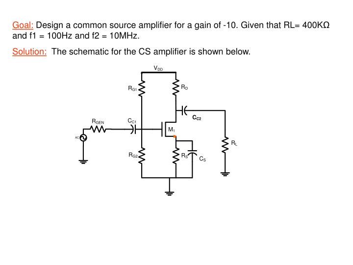
Goal: Design a common source amplifier for a gain of -10. Given that RL= 400K Ω and f1 = 100Hz and f2 = 10MHz. Solution: The schematic for the CS amplifier is shown below. Step1: Select an appropriate Q point for the Device.

E N D
Goal:Design a common source amplifier for a gain of -10. Given that RL= 400KΩ and f1 = 100Hz and f2 = 10MHz. Solution: The schematic for the CS amplifier is shown below.
Step1: Select an appropriate Q point for the Device. • There can be various constraints on selecting the Q point of the device . • If there is a power constraint that is to be met , then Vdd X Id = Pdiss ID < Pdiss/Vdd • Since this constraint is not mentioned , for this problem , I will choose the following: • VDSQ = 4V, ID = 1mAVDSQ >approx VDD/3 to VDD/2
In general VDD = ID.RD+ VDSQ+ID.RS (1) If VDSQ = VDD/2 (2) IDD < (3) Step2: Determine Rs from the ID Vs. VGS curve of the given Mosfet. (4) From the above curve Rs = 2KΩ.
Step3: Determine RD from the given gain specification. The Dc gain of the given circuit can be expressed as -gm(RDIIroIIRL) = -10 (5) • Since we have chosen the required current , ro can be calculated from (6) • If λ is not mentioned it can be calculated from the given ID –VDS curves of the transistor. • gm can be calculated from ID Vs.Vgs curve of the device as (7)
If RD << ro,RL eq can be expressed as -gm x RD = -10 Assuming gm = 1mS , RD can be calculated to be equal to 10KΩ. (5) Step4:Determine the required VGG VGG = VGS + ID RS = 3 V + 1mA 2K = 5V (8) The value of VGS was chosen from curve 1. Step5: (9) chose RG = RG1II RG2 >> Rgen Rgen for most instruments is 50Ω, choosing RG1 = RG2 = 10KΩ gives RG = 5KΩ and VGG = 5V .
Step6:From the small signal model of the amplifier , determine the poles
The following are the “f1” poles of the circuit. Cc1> 3.15µF, choose CC1 = 4.7µF. Cs> 8µF ,choose Cs = 10µF. CC2> 38nF, choose Cc2 = 47nF.
The following are the “f2” poles of the circuit. CL < 3pF , choose or Make sire that is CL < 3pFor Is selected at CL= 2pF When using a discrete device , check data sheet to make sure CISS meets the criteria for P5.