Download
1 / 46
470 likes | 523 Views
DIODES. Celso José Faria de Araújo, Dr. The ideal diode: (a) diode circuit symbol; (b) i-v characteristic; (c) equivalent circuit in the reverse direction; (d) equivalent circuit in the forward direction.

E N D
DIODES Celso José Faria de Araújo, Dr.
The ideal diode: (a) diode circuit symbol; (b) i-v characteristic; (c) equivalent circuit in the reverse direction; (d) equivalent circuit in the forward direction. Diodes Electronics – Celso José Faria de Araújo, M.Sc.
(a) Rectifier circuit. (b) Input waveform. (c) Equivalent circuit when (d) Equivalent circuit when v1 0 (e) Output waveform. Diodes Electronics – Celso José Faria de Araújo, M.Sc.
Examples (Ideal Diode) DIODE LOGIC GATES BATTERY-LOAD CIRCUIT (vS sinusoidal) The current iD flew to battery through diode at 20% of input signal period whose mean value is 100mA. (a)Vpp = ? (b) R=? (c) ID(Peak) = ? Diodes Electronics – Celso José Faria de Araújo, M.Sc.
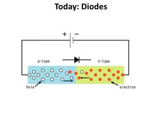
Simplified physical structure of the junction diode. Diodes Electronics – Celso José Faria de Araújo, M.Sc.
(a) The pn junction with no applied voltage (open-circuited terminals). (b) The potential distribution along an axis perpendicular to the junction. Diodes Electronics – Celso José Faria de Araújo, M.Sc.
(a) The pn junction excited by a constant-current source I in the reverse direction. To avoid breakdown, I is kept smaller than Is. Note that the depletion layer widens and the barrier voltage increases by Vr volts, which appears between the terminals as a reverse voltage.(b) The pn junction excited by a constant-current source supplying a current I in the forward direction. The depletion layer narrows and the barrier voltage decreases by Vvolts, which appears as an external voltage in the forward direction. (b) (a) Diodes Electronics – Celso José Faria de Araújo, M.Sc.
The diode i-v relationship with some scales expanded and others compressed in order to reveal details. Diodes Electronics – Celso José Faria de Araújo, M.Sc.
The Forward-Bias Region IS = Saturation CurrentIS is a constant for a given diode at a given temperature. It’s also called Scale Current due to fact that IS is directly proportional to the cross-sectional area of de diode. IS is of the order of 10 –15 A. VT = Thermal Voltage k = Boltzmann’s constant = 1.38x10 –23Joules/Kelvin T = the absolute temperature in Kelvin q = the magnitude of electronic charge = 1.60x10 –19 Coulomb VT(20 o)=25.2mV 25mV 1 n 2 n=1 standard integrated-circuit and n=2 discrete two-terminal components. Diodes Electronics – Celso José Faria de Araújo, M.Sc.
Graph of i-v characteristic of a p-n junction diodeIS=1x10-15A, n=1 and VT=25mV Diodes Electronics – Celso José Faria de Araújo, M.Sc.
Diode i-v characteristic on semilog scale Diodes Electronics – Celso José Faria de Araújo, M.Sc.
Example: Area x Scale Current Diodes Electronics – Celso José Faria de Araújo, M.Sc.
Temperature Effect Forward – Bias Region Reverse – Bias Region IS doubles for every 10oC in temperature. Diodes Electronics – Celso José Faria de Araújo, M.Sc.
Exercises (1) • Consider a silicon with n=1.5. Find the change in voltage if current changes from 0.1mA to 10mA. Ans. 172.5mV • A silicon junction diode with n=1 has v=0.7V at i=1mA. Find the voltage drop at i=0.1mA and i=10mA. Ans. 0.64V; 0.76V • Using the fact that a silicon diode has IS=10-14A at 25oC and that IS increases by 15% per oC rise in temperature, find the value of IS at 125oC. Ans. 1.17x10⁻⁸A • The diode in the circuit of figure below is a large, high-current device whose reverse leakage is reasonably independent of voltage. If V=1V at 20oC, find the value of V at 40oC and at 0oC. Ans. 4V; 0.25V Diodes Electronics – Celso José Faria de Araújo, M.Sc.
Exercises (2) • For the circuit shown below, both diodes are identical, conducting 10mA at 0,7V and 100mA at 0,8V. Find the value of R, for which V = 50mV. • In the circuit shown below, both diodes have n = 1 , but D1 has ten times the junction area of D2. What value of V results for ID1of 1mA? To obtain a value for V of 50mV, what current ID1 is needed? • A junction Diode is operated in a circuit in which it is supplied with a constant current I. What is the effect on the forward voltage of the diode if an identical diode is connected in parallel? Assume n= 1. Diodes Electronics – Celso José Faria de Araújo, M.Sc.
Graphical Analysis Diodes Electronics – Celso José Faria de Araújo, M.Sc.
Iterative Analysis Determine the current ID and the diode voltage VD for the circuit below with VDD=5V and R=1k. Assume that the diode has a current of 1mA at a voltage of 0.7V and that its voltage drop changes by 0.1V for every decade change in current. Recurrent Equation: To begin the iteration, we assume that VD=0.7V Diodes Electronics – Celso José Faria de Araújo, M.Sc.
Piecewise-linear Model of the diode forward characteristic and its equivalent circuit representation. Diodes Electronics – Celso José Faria de Araújo, M.Sc.
Example of Piecewise-linear model of the diode forward characteristic. Determine the current ID and the diode voltage VD for the circuit below with VDD=5V and R=1k, utilizing the piecewise-linear model whose parameters are given in figure below. VDO = 0.65V rD=20 Diodes Electronics – Celso José Faria de Araújo, M.Sc.
The constant-voltage-drop model of the diode forward characteristic and its equivalent circuit representation. Determine the current ID and the diode voltage VD for the circuit below with VDD=5V and R=1k, utilizing the constant-voltage-drop model (VDO= 0.7V). Diodes Electronics – Celso José Faria de Araújo, M.Sc.
Exercises (3) • For the circuits in Fig. below find ID and VD for the case VDD=5V and R=10K. Assume that the diode has a voltage of 0.7V at 1mA current that voltage changes by 0.1V/decade of current change. Use (a) iteration (b) the piecewise-linear model with rD=20 and (c) the constant-voltage-drop model with VD=0.7V. Ans. (a) 0.434mA, 0.63V; (b) 0.431mA, 0.689V; (c) 0.43mA, 0.7V. • Consider a diode that is 100 times as large (in junction area) as a diode whose characteristics are VDO=0.65V and rD=20 how would the model parameters VDO and rD change? Ans.VDO does not change; rD decreases by a factor of 100 to 0.2V. • Design the circuit in figure below to provide an output voltage of 2.4V. Assume that the diodes available have 0.7V drop at 1mA and that V=0.1V/decade change in current. Ans. 760 . Diodes Electronics – Celso José Faria de Araújo, M.Sc.
Development of the diode small-signal model.Note that the numerical values shown are for a diode with n = 2. rd is a small-signal resistance or incremental resistance Equivalent circuit model for the diode for small changes around bias point Q. The incremental resistance rd is the inverse of the slope of the tangent at Q, and VD0 is the intercept of the tangent on the vD axis. Diodes Electronics – Celso José Faria de Araújo, M.Sc.
The analysis of the circuit in (a), which contains both dc and signal quantities, can be performed by replacing the diode with the model of Fig. (a), as shown in (b). This allows separating the dc analysis [the circuit in (c)] from the signal analysis [the circuit in (d)]. (a) (b) (c) (d) Diodes Electronics – Celso José Faria de Araújo, M.Sc.
Example of using small-signal model (1) • Consider the circuit shown in fig. below for the case R=10K. The power supply V+ has a DC value of 10V on which is superimposed a 60Hz sinusoid of 1V peak amplitude (power supply ripple). Calculate both the DC voltage of the diode and the amplitude of the sine-wave signal appearing across it. Assume the diode to have a 0.7V drop at 1mA current and n=2. Diodes Electronics – Celso José Faria de Araújo, M.Sc.
Example of using small-signal model (2) • Consider the circuit shown in fig. below. A string of three diodes is used to provide a constant voltage of about 2.1V. We want to calculate the percentage change in this regulated voltage caused by (a) 10% change in the power-supply voltage and (b) connection of a 1K load resistance. Assume n = 2. (b) For all three diodes the small-signal model we can use the parameters VDO=1.95V and rd= 18.9 obtained from (a) analysis. Diodes Electronics – Celso José Faria de Araújo, M.Sc.
Exercises (4) • Find the value of the diode small-signal resistance at bias current of 0.1, 1, and 10mA. Assume n=1. Ans. 250; 25; 2.5. • For a diode that conducts 1mA at a forward voltage drop of 0.7V and whose n=1, find the equation of the straight-line tangent at ID=1mA. Ans.iD = (1/25)(vD-0.675). • Consider a diode with n=2 biased at 1mA. Find the change in current as a result of changing the voltage by (a) –20mV; (b) –10mV; (c) -5mV (d) +5mV (e)+10mV; (f) +20mV. In each case, do the calculations (i) using the small-signal model and (ii) using the exponential model. Ans. (a) –0.40, -0.33mA; (b) –0.20, -0.18mA; (c) –0.10, -0.10mA; (d) +0.10, +0.11mA; (e) +0.20, +0.22mA; (f) +0.40, +0.49mA. • Design the circuit of fig. below so that VO=3V when IL= 0, and VO changes by 40mV per 1mA of load current. Find the value of R and the junction area of each diode (assume all four diodes are identical) relative to a diode with 0.7V drop at 1mA current. Assume n=1. Ans.R= 4.8k; 0.34. Diodes Electronics – Celso José Faria de Araújo, M.Sc.
Operation in the Reverse Breakdown Region-Zener Diodes. Model for the zener diode. Circuit symbol for a zener diode. The diode i-v characteristic with the breakdown region shown in some detail. Diodes Electronics – Celso José Faria de Araújo, M.Sc.
Design of the Shunt Regulator Diodes Electronics – Celso José Faria de Araújo, M.Sc.
Zener Diode - Example The 6.8V zener diode in the circuit of fig. below is specified to have VZ = 6.8V at IZ = 5mA, rz = 20, and IZK= 0.2mA. The supply voltage V+ is nominally 10V but can vary by 1V. (a) Find VO with no load and with V+ at its nominal value. (b) Find the change in VO resulting from the 1V change in V+. (c) Find the change in VO resulting from connecting a load resistance RL = 2k. (d) Find the value of VO when RL = 0.5k. (e) What is the minimum value of RL for which the diode still operates in the breakdown region? Diodes Electronics – Celso José Faria de Araújo, M.Sc.
Block Diagram of a DC Power Supply. Diodes Electronics – Celso José Faria de Araújo, M.Sc.
(a) Half-wave rectifier. (b) Equivalent circuit of the half-wave rectifier with the diode replaced with its battery-plus-resistance model. (c) transfer characteristic of the rectifier circuit. (d) Input and output waveforms, assuming that rD<< R. Diodes Electronics – Celso José Faria de Araújo, M.Sc.
Full-wave rectifier utilizing a transformer with a center-tapped secondary winding. (a) Circuit. (b) Transfer characteristic assuming a constant-voltage-drop model for the diodes. (c) Input and output waveforms. Diodes Electronics – Celso José Faria de Araújo, M.Sc.
The bridge rectifier: (a) circuit and (b) input and output waveforms. Diodes Electronics – Celso José Faria de Araújo, M.Sc.
Voltage and current waveforms in the peak rectifier circuit with CR >> T. The diode is assumed ideal. (Half Wave) Diodes Electronics – Celso José Faria de Araújo, M.Sc.
Voltage and current waveforms in the peak rectifier circuit with CR >> T. The diode is assumed ideal. (Full Wave Rectifier) Diodes Electronics – Celso José Faria de Araújo, M.Sc.
Exercises (5) • Consider a bridge-rectifier circuit with a filter capacitor C placed across the load resistor R, for the case in which the transformer secondary delivers a sinusoid of 12 Vrms having 60Hz frequency, and assuming VDO= 0,8 V and a load resistance R= 100 . Find the value of C that results in a ripple voltage no larger than 1 Vpp. What is the DC voltage at the output? Find the load current. Find de diodes conduction angle. What is the average diode current? What is the peak reverse voltage across each diode? Specify the diode in terms of its peak current and its PIV. Ans. 1281F; 15.4V or (a better estimate) 14.9V; 0.15A; 0.36 rad; 1.45A; 2.74A; 16.2V. Thus select a diode with 3.5 to 4 A peak current and a 25 V PIV rating (50%). • It is required to use a peak rectifier to design a DC power supply that provides an average DC output voltage of 15V on which a maximum of 1V ripple is allowed. The rectifier feeds a load of 150. The rectifier is fed from the line voltage (120Vrms – 60Hz) through a transformer. The diodes available have 0.7V drop when conducting. If the designer opts for the half-wave circuit: (a) Specify the rms voltage that must appear across the transformer secondary. (b) Find the required value of the filter capacitor. (c) Find the maximum reverse voltage that will appear across the diode, and specify the PIV rating of the diode. (d) Calculate the average current through the diode during conduction. (e) Calculate the peak diode current. Ans. (a) 11.8Vrms; (b) 889F; (c) 32.7V; (d) 2.61A; (e) 1.36 A. Diodes Electronics – Celso José Faria de Araújo, M.Sc.
A VARIETY OF BASIC LIMITING CIRCUITS. Diodes Electronics – Celso José Faria de Araújo, M.Sc.
Exercises (6) • Assuming the diodes to be ideal, describe the transfer characteristic of the circuits shown in Figure below. • Assuming the diodes has a 0.7V drop when conducting and the zener specified voltage is 8.2V (ideal), describe the transfer characteristic of the circuits shown in Figure below. Diodes Electronics – Celso José Faria de Araújo, M.Sc.
The Clamped Capacitor or DC Restorer Determine VX to have an average voltage of output “A” for the circuit shown in figure below. Consider the diode ideal and the input signal is that shown in figure below. Ans.: VX = -(1/2)A V Diodes Electronics – Celso José Faria de Araújo, M.Sc.
The Voltage Doubler Diodes Electronics – Celso José Faria de Araújo, M.Sc.
SPECIAL DIODES TYPES • The Schottky-Barrier Diode (SBD) • Varactors • Photodiodes • Light-Emitting Diodes (LEDs) Diodes Electronics – Celso José Faria de Araújo, M.Sc.
Photonic DevicesLight-emitting diodes (LED) recombination electron (+) hole (-) • heat • light (E=h) energy = EG / h h:Planck’s constant h=6.63x10⁻³⁴ Jsec Materials: GaAs ( infrared ) GaAs1-xPx GaAs0.6P0.4 red light ( EG 1.8 eV ) B.G. Streetman, Solid State Electronic Devices, 2nd edition, Prentice-Hall, 1980 Diodes Electronics – Celso José Faria de Araújo, M.Sc.
Photodiodes (1/2) h > EG Gop: optical generation rate Relative number of MINORITY carriers increase by a large amount drift current increases. Diodes Electronics – Celso José Faria de Araújo, M.Sc.
i D No illumination a V v OC D b c I SC Photodiodes (2/2) a,c p = vD x iD > 0 b p = vD x iD < 0 the diode is a power source. Model for optically illuminated diode. iPH represents the current generated by absorption of photons in the vicinity of the pn junction. Diodes Electronics – Celso José Faria de Araújo, M.Sc.
Photodetector Optoisolator • Light-to-voltage converter No illumination: VO = VB Illumination: VO = VB - Riph Diodes Electronics – Celso José Faria de Araújo, M.Sc.
3 in Solar cells V = Vm , I = Im for P = Pmax VmIm < VocIsc Average solar energy (zenith): 100mW/cm2 Maximum power 300 mW Efficiency of solar cells range between 10% and 20% Diodes Electronics – Celso José Faria de Araújo, M.Sc.