Download
1 / 13
160 likes | 1.24k Views
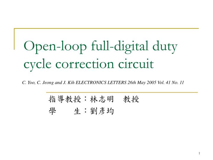
Open-loop full-digital duty cycle correction circuit. C. Yoo, C. Jeong and J. Kih ELECTRONICS LETTERS 26th May 2005 Vol. 41 No. 11. 指導教授:林志明 教授 學 生:劉彥均. Outline. Introduction Open-loop full digital duty cycle correction Experimental result Conclusion References. Introduction.

E N D
Open-loop full-digital duty cycle correction circuit C. Yoo, C. Jeong and J. Kih ELECTRONICS LETTERS 26th May 2005 Vol. 41 No. 11 指導教授:林志明 教授 學 生:劉彥均
Outline • Introduction • Open-loop full digital duty cycle correction • Experimental result • Conclusion • References
Introduction • Utilising both ring and falling edges of the clock, data transfer rate can be doubled. • 50% duty cycle desired, otherwise valid data window&operable data rate are decreased. • Distorted, imperfections of the clock buffer.
Introduction • DCC control information must be stored as digital code, two approach have been proposed so far: (1) Two matched DLL and interpolator[2]. (2) Two matched delay lines[3]. (Complicated control scheme and additional power consumption due to the closed loop architecture)
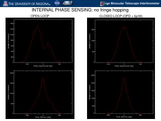
Open-loop full digital duty cycle correction a. Timing diagram of open-loop full-digital DCC
Open-loop full digital duty cycle correction b. Block diagram of open-loop full-digital DCC
Open-loop full digital duty cycle correction Simulated output waveform of DCC at 600 MHz with 10% input duty error
Open-loop full digital duty cycle correction • The total delay of delay line should be grater than the HIGH duration of the input clock. • Smaller unit delay, better accuracy of inpolation. • Trade-off between the accuracy and area/power consumption.
Experimental result Measured jitter histogram of DCC output at 600 MHz
Experimental result Measured DCC accuracy
Experimental result waveform of output clock for clock frequency of 600 MHz and input duty cycle of 40%
Conclusion • Measure accuracy is 0.8% for 10% input clock error. • Be corrected within five clock cycles. • Turn-off during the power-down state. • Implemented in a 0.35 CMOS process.
References [1] Lee, T.H., Donnelly, K.S., Ho, J.T.C., Zerbe, J., Johnson, M.G., and Ishikawa, T.: ‘A 2.5 V CMOS delay locked loop for 18 Mbit, 500 megabyte=s DRAM’, IEEE J. Solid-State Circuits, 1994, 29, (12), pp. 1491–1496 [2] Lee, J.-B., Kim, K.-H., Yoo, C., Lee, S., Na, O.-G., Lee, C.-Y., Song, H.-Y., Lee, J.-S., Lee, Z.-H., Yeom, K.-W., Chung, H.-J., Seo, I.-W., Chae, M.-S., Choi, Y.-H., and Cho, S.-I.: ‘Digitally-controlled DLL and I=O circuits for 500 Mb=s=pin 16 DDR SDRAM’. Dig. Tech. Pprs, ISSCC, 2001, San Francisco, CA, USA, pp. 68–69 [3]Matano, T., Takai, Y., Takahashi, T., Sakito, Y., Fujii, I., Takahashi, Y.T., Fujisawa, H., Kubouchi, S., Narui, S., Arai, K., Morino, M., Nakamura, M., Miyatake, S., Sekiguchi, T., Koyama, K., and Miyazawa, K.: ‘A 1-Gb=s=pin 512-Mb DDRII SDRAM using a digital DLL and a slewrate- controlled output buffer’. Dig. Tech. Pprs, VLSI Circuits Symp., 2002, pp. 112–113