Download
1 / 22
220 likes | 331 Views
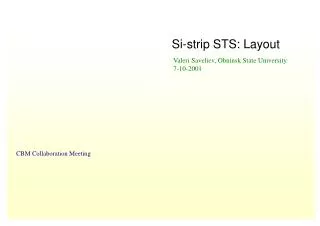
Si-Strip Tracker of CBM Experiment at GSI, Darmstadt. Valeri Saveliev, Obninsk State University for Si-Strip STS Collaboration. CBM Coordination Meeting, Moscow, Russia, 5.11.2005.

E N D
Si-Strip Tracker of CBM Experiment at GSI, Darmstadt Valeri Saveliev, Obninsk State University for Si-Strip STS Collaboration. CBM Coordination Meeting, Moscow, Russia, 5.11.2005 CBM Coordination Meeting
Si-Strip STS Collaboration CKBM, St.Petersburg Si-STS design, construction aspects and technology Moscow Engineering and Physics Institute (University) Front end electronics and readout electronics Moscow State University, Si sensors design and technology, front end and readout electronics Obninsk State University, Si-STS system design, Monte Carlo simulation and analysis, Physics V.G.Khlopin Radium Institute, St.Petersburg, Si-STS design, Construction aspects, Radiation hardness test. CBM Coordination Meeting
Main features for Si-Strip STS in CBM Experiment • Extremely High Multiplicity, • Importance of Material Budget, • Requirement of High Resolutions. Schematic View of Geometry of the Si-Strip STS 4 Si-Strip Planes inside the Magnet (equivalent distances along z, starting 40 cm from Target ) Si-Strip STS CBM Coordination Meeting
Obninsk State University Good experience in Monte Carlo and Analysis for High Energy Physics Experiments Monte Carlo Simulation and Analysis Monte Carlo Event simulation of Central Collisions of Au+Au 25 AGeV CBM Coordination Meeting
Total and Radial Occupancy of Si-Strip STS: STS_4, STS_5, STS_6, STS_7 (Si-Strip Sensors 100 mm, no Mechanics Construction, no Support Structure) Radial Occupancy of Si-Strip STS and problem of secondary particles limited of use the Si-Strip Thechnology in location close 40 cm from Target Occupancy of Si-Strip STS STS_4 STS_5 STS_6 STS_7 STS_4 STS_5 STS_6 STS_7 CBM Coordination Meeting
Double Sided Si-Strip Detectors Thickness : 100 mm Pitch of strips : 25 mm Stereo Angle : 15o Outer region of the Si-Strip STS: Long Lader Technology Inner region of Si-Strip STS: According the occupancy for STS_4: 4.2% for 2 cm length of strip Basic Technology of Si-Strip STS Sensors are 4’’ , 300 µ thick, double-sided, 70 × 40.1 mm2, 110 µ/208µ readout pitch A set of strips are connected in serpentine; thus strips with following length: 28 cm, 56 cm, 112 cm and 224 cm are tested (SiILC Collaboration). CBM Coordination Meeting
Basic Elements: Inner : 6x2 cm Middle : 6x4 cm Outer : 6X12 cm Si strip STS_4 Layout +20 cm -20 cm Read out CBM Coordination Meeting
Basic Elements: Inner : 6x4 cm Middle : 6x12 cm Outer : 6X20 cm Si strip STS_6 Layout +40 cm +4cm - 4cm -40 cm Read out CBM Coordination Meeting
Moscow State University 15 years experience in Si Sensors Design and Production; V.G.Khlopin Radium Institute, St.Petersburg Si-Detectors Design and Radiation Hardness Test Si-Sensores Development Status • Experience in double side photolithography, first prototype for ATLAS SCT; • Good new mask aligner for double side photolithography up to 6” • Fine pitch (up to 25 mm) sensors have been designed and produced for SVD-2 experiment at IHEP, Protvino; • Radiation hard sensors designed, prototypes produced and tested up to 8 MRad for D0 RunIIb; • Almost all equipment for Si-sensors testing. CBM Coordination Meeting
Test Station for Characterisation of Si-Strip Sensors Si-Sensores Development Status • Light protective box • MKD light microscope • Control and data acquisition electronic modules • Software CBM Coordination Meeting
First of lall: Thickness of Si-Strip Sensors No well defined technology for 100 mm thickness of Si-Strip Sensors up to now Long Lader Technology for Double Sided Si-Strip Sensors Si-Sensors R&D is necessary CBM Coordination Meeting
Si-Sensors R&D Double side polished silicon wafers: • 300 µm – 25 wafers (for tests only) • 200 µm – 50 wafers; (for prototype • 150 µm – 50 wafers. production) Total Wafers Cost – 4000 ÷ 6000 Euro (Depends on Resistivity and Suplier) Photomasks design and production. For Double Side Sensors we need 14 or 15 photomasks. • Cost about 500 - 600 Euro/mask Total Masks Production: 7000 ÷ 9000 Euro Sensor production cost (prototypes): • 300 µm – 600 €/wafer; • 200 µm – 700 €/wafer; • 150 µm – 800 €/wafer. This is not a sensor cost !!! It might be a lot of sensors on wafer, total active area ~36 cm2 Cost of Production of Prototypes(~50 wafers) 35 000 Euro CBM Coordination Meeting
Si-Sensores R&D Time Schedule Photomasks design and production - 3 months; Sensor prototype production: • 300 µm – 10÷15 wafers - 4 months; • 200 µm – first 10 wafers - 4 months; • 200 µm – second 10 wafers – 2 months; • 150 µm – first 10 wafers -3 months; • 150 µm – second 10 wafers -2 months; In total according this optimistic schedule we will have about 50 wafers with different sensors in 12 – 14 months. Two last months mainly for testing sensors. Radiation tests could be started on the first batches of 10 sensors. CBM Coordination Meeting
Si-Strip STS Readout • The main aim of the ASIC to be developed for CBM Si-Strip detectors is to provide both amplitude and timing (event separation) measurements • Mechanical (dimensional) fit (face-to-face) between strips and caseless ASICs • Space limitation at the detector forces to provide reasonable multiplexing to save a number of cables (communication lines) to be used • Data Driven Architecture (The Self-Triggering is an important issue) • Accurate track reconstruction forces to have: • Massive parallelism of read-out • High complexity (functionality) of mixed-signal ASICs • Radiation hardness (tolerance) Si-Strip STS Readout is can’t be unified with other CBM Spectrometer System Readout CBM Coordination Meeting
Moscow Engineering and Physics Institute, Moscow State University Experience in the Readout Development for large scale Experiments in High Energy Physics Si-Strip STS Readout Status MEPhI is Europractice full membership number A47530 Access to modern technology development • PCs and Sun Workstations • Linux and Solaris environment • Cadence tools • Europractice Design Kits • ISE CBM Coordination Meeting
Si-Strip STS Frontend • Minimal signal – 7000 electrons per mip (100um detector thickness) • Detector capacitance can be 30-300 pF depending on thickness and length of the strip, as follows from the simulation and design of tracker at a suitable signal/noise ratio • Signal noise ratio – better than 10 for 1 mip • Dynamic range (?) – 10 mips • Input signals come at random time. Maximal average frequency of the signal at the chip input is 10 MHz • Radiation hardness – 15-20 MRad • Power consumption, as small as possible. The maximal one – few mW/channel • Supply voltages depend on the technology • Number of channels on the chip is dictated by tracker design (128, 256,….) • Minimal number of external components. CBM Coordination Meeting
Si-Strip STS Technology Choice • “Today 0.13-0.25CMOS processes form the mainstream industrial production technologies and 0.13 um processes are coming on-line as the next industrial generation” (P. Jarron. Trends in microelectronics and nanoelectronics and their impact on HEP instrumentation. Proc. of the 8th Workshop on Electronics for LHC experiments, 9-13 Sept. 2002, Colmar, CERN/LHCC-2002-034, p.9-16) • Probably it is expedient to add 0.25…0.35 µm Bi-CMOS processes. Bipolar is dictated by precise analog blocks (like low-offset comparators, erational amplifiers etc) • Radiation tolerant Deep Sub Micron (DSM) 0.13 (0.25??) mm CMOS process (0.25 - 0.35 mm Bi-CMOS one) for prototyping and studying the possibilities seems to be the best candidate and recommended last meeting at CERN Oct.24-26 CBM Coordination Meeting
Si-Strip STS Readout R&D Fabrication cost of prototype ASICs (given by e.g. Europractice) It strongly depends on the process. (Currently Europractice discounted prices are 240…7500 € /mm2 type.) The mass (more correctly to say small volume) production cost should be comparable with prototyping cost. 1.5*106 channels ~100 channels/chip & ~1000chips/wafer ~15 wafers only! Designer man-power cost. It is roughly 2..4 man*year per each prototype ASIC Man power cost of test electronics development is about 1..2 man*year per each prototype ASIC On the way costs for computing (hard and soft) are estimated as a few k€/year Other costs include mechanical design (PCBs), assemblage and their tests CBM Coordination Meeting
Option 1 Polarity Switch Input protection CR-RC(n) Shaper (n=2) Soft Limiter Scale amplifier CSA To ADC Ccal Limitation adjustment Feedback adjustment Peak time adjustment Gain adjustment Switch array Fast shaper T-Pulse DAC array Analog finder Test data DAC Threshold Calibration (test) System CBM Coordination Meeting
Option 1 Pedestal Subtraction Data reduction Noise reduction Zero suppression ADC Buffer Pedestal memory Shape reconstruction Interface (serial) Amplitude Time reconstruction Pedestal calculator Signal finder Internal Pulser (phase control) Pedestal Measurement Mode External CLK Control CBM Coordination Meeting
CKBM, St.Petersburg Leader of high tech Carbon Composite Material Technology and Design of Mechanics Structures, well known in High Energy Physics: participating in the large scale projects of LHC Si-Strip STS Mechanics Structure • Starting of the design on base preliminary Si-Strip STS Layout • Actually technology is exists, but of course should be taking to account CBM specific items. CBM Coordination Meeting
Summary Si-Strip STS R&D 2005 • Full Monte Carlo Analysis of Si-Strip STS in common simulation frame of CBM Experiment for optimisation of Design and Layout. Implementation of the Si-Strip STS in Physics Simulation Analysis. • Study and Development of the technology for Double Sided Si-Strip Sensors with thickness of 100 mm. Study and Analysis of Long Lader technology for outer part of the Si-Strip STS. • Analysis and Development of the Structure of the Readout Chain of Si-Strip STS with emphasis of Data Driven Apchitecture. Design of specific Analog Front end part for the thin Si-Strip sensors, including the prototyping for the test setup of Si-Strip Sensors. Budget: R&D Si-Sensors and Readout ~150 kEuro for 2005 GSI visits ath the level of 24 man*months CBM Coordination Meeting