Download
1 / 28
410 likes | 1.47k Views
Transistor-Transistor Logic and BiCMOS. Dr. T.Y. Chang NTHU EE 2007.12.11_13. Introduction. Diode-Transistor Logic Basic TTL NAND gate Schottky TTL BiCMOS Text Book: D.A. Neamen, Electronic Circuits Analysis And Design, 2nd ed. Chapters 17. Parameters. Diode-Transistor Logic.

E N D
Transistor-Transistor Logic and BiCMOS Dr. T.Y. Chang NTHU EE 2007.12.11_13
Introduction • Diode-Transistor Logic • Basic TTL NAND gate • Schottky TTL • BiCMOS Text Book:D.A. Neamen, Electronic Circuits Analysis And Design, 2nd ed. Chapters 17.
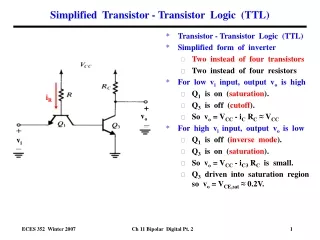
Diode-Transistor Logic Logic-1=5V Logic-0=0.1V
Example 17.8 @p1137 • Find Is and Vs in DTL as shown in Fig. 17.20 with =25.
TTL Ex 17.9 Find Is, Vs, and Max. Fanout of Fig. 17.24. R=0.1, =25. • If No Rc Called • Open-Collector TTL (OC TTL) • Wired-AND: • Connects outputs of OC TTLs • and adds an Rc
Tristate Output =0 switch open =1 switch on
Example 17.12 @p1154 • Calculate power dissipation in Fig. 17.34 with =25, V=0.7V, VCE(sat)=0.4V.
BiCMOS • CMOS • Low Power • Slower • BJT • Faster • High Power • Core: CMOS, Interface: BJT
Basic BiCMOS Inverter • Totem-Pole Configuration (Q1-Q2) • Turn-off time • VOH=VDD-VBE(ON) • VOL=VBE(ON) 1 0
BiCMOS Inverters =0V or = VDD =VBE(ON) or = VDD VBE(ON)
BiCMOS Inverter I • Reduce Turn-off time • “bleeder resistors” R1 and R2 are added • VOH=VDD-VBE(ON) • VOL=VBE(ON)
BiCMOS Inverter II • Reduce Turn-off time • VOH=VDD and VOL=0
Problem (Not HW) • Implement E=AB+CD in two-level TTL gates. • Implement a BiCMOS NAND gate.
Solutions • E=AB+CD =((AB)’ (CD)’)’