Download
1 / 55
670 likes | 1.05k Views
KeyStone ARM Cortex A-15 CorePac Overview. KeyStone Training Multicore Applications Literature Number: SPRP804. Agenda. ARM CorePac in KeyStone II ARM Cortex A-15 Features Interface to the SOC and Coherency Issues Benchmarks Interrupt Controller Power Management Debug and Trace.

E N D
KeyStoneARM Cortex A-15 CorePac Overview KeyStone Training Multicore Applications Literature Number: SPRP804
Agenda ARM CorePac in KeyStone II ARM Cortex A-15 Features Interface to the SOC and Coherency Issues Benchmarks Interrupt Controller Power Management Debug and Trace
ARM CorePac in KeyStone II ARM Cortex A-15 CorePac Overview
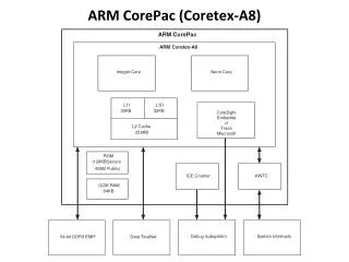
KeyStone II and ARM CorePac (1/2) Single, Dual, or Quad-ARM Cortex A15 CorePac operating at up to 1.4 GHz. L1 Memory: 32KB L1 Data cache 32KB L1 Program Cache Up to 128-bit access 64-byte L1 D cache line (up to 6 outstanding requests) L2 Memory: 4 MB L2 Cache is shared between the 1 to 4 ARM A-15 core(s) 4 tag banks 4 data banks 64-byte cache line
KeyStone II and ARM CorePac (2/2) AMBA 4.0 AXI Coherency Extension (ACE) master port Module interrupt controller Cluster-level and core-level power management and low-power standby modes Configured 64/128-bit AMBA interface and 64/128-bit Accelerator Coherency Support (ACP) Advance debug features
ARM Cortex A-15 Features:ARM Core ARM Cortex A-15 CorePac Overview
Cortex A-15 Features: ARM Core (1/2) • Superscalar architecture: • 2 ALU, 2 shifts, branch unit, multiply and divide, load store • 3 concurrent decoded, up to 8 concurrent issues • Full implementation of ARMv7-A architecture instruction set: • More MAC instructions (normalization and rounding) • Integer divide • Automatic thumb mode (16-bit instructions) • Pipeline optimization: • Deeper pipeline, 13 stages to issue (2 integer, 4 multiply and load, more for NEON and FPU(2-10)) • Out-of-order pipeline (3-12 stages) execution
Cortex A-15 Features: ARM Core (2/2) • Dynamic branch prediction – Loop prediction and indirect branch predictor • Branch Target Buffer (BTB) • Global History Buffer (GHB) has three arrays: • Taken array • Not taken array • Selector array • Sophisticated hardware algorithm makes the prediction
Cortex A-15 Features: Fetch & Memory • Increase fetch from 64 to 128 bits • Full support for unaligned fetch address • L1D and L1P: • 32KB size • Configured as cache • L2 is unified memory that serves ALL cores in the cluster: • 4MB size • Configured as cache
ARM Cortex A-15 Features:NEON ARM Cortex A-15 CorePac Overview
SIMD Engine NEON • 64/128-bit data instructions • Fully integrated into the main pipeline • 32x 64-bit registers that can be arranged as 128-bit registers • Data can be interpreted as follows: • Byte • Half-word (16-bit) • Word • Long
NEON Registers NEON registers load and store data into 64-bit registers from memory with on-the-fly interleave, as shown in this diagram. Source: ARM Compiler Toolchain Assembler Reference; DUI0489C
ARM Cortex A-15 Features:Vector Floating Point (VFP) ARM Cortex A-15 CorePac Overview
Vector Floating Point (VFP) Fully integrated into the main pipeline 32 DP registers for FP operations Native (hardware) support for all IEEE-defined floating-point operations and rounding modes; Single- and double-precision Supports fused MAC operation (e.g., rounding after the addition or after the multiplication) Supports half-precision (IEEE754-2008);1-bit sign, 5-bit exponent, 10-bit mantissa
ARM Cortex A-15 Features:Memory Management Unit (MMU) ARM Cortex A-15 CorePac Overview
Memory Management Unit (MMU) • Logical-to-physical memory translation: • User protected • Hardware manages the actual memory • Large physical addressing; 40-bit (1TB) • Three-level data structure for virtual 4kB page: • Two levels for virtual 2MB pages (Linux huge pages) • Translation Lookaside Buffers (TLB) cache one page of address translations per entry to speed up the translation process: • L1 instruction access • L1 data access • L2 TLB
MMU, TLB, and Page Memory … Page 1 CorePac MMU Logical Address Physical Address Page 2 Page 3 Page 4 TLB Page 5
Memory Management Unit (MMU) To support multiple operating systems (adding a Guest operating system): • Three privilege layers: • User Mode is for “Guest” (application) • Supervisor controls multiple guests • Hypervisor controls the complete system • Two-stage translation: • From logical to intermediate physical address for supervisor for each operating system • From intermediate to real address for hypervisor for the complete system
Two-Stage MMU: Stage One Source: Virtualization is Coming to a Platform Near You
Two-Stage MMU: Stage Two Source: Virtualization is Coming to a Platform Near You
Interface to the SOC andCoherency Issues ARM Cortex A-15 CorePac Overview
ARM Cluster BusesAMBA – Advance Microcontroller Bus Architecture AXI (AMBA Advanced eXtensible Interface) connects the ARM cluster with MSMC module using the AXI-VBUS master. APB (AMBA Advanced Peripheral Bus) provides access to peripherals and internal memories. ATB (AMBA Trace Bus) supports the trace features for the ARM cluster.
ARM AXI-VBUSM Interfaces to the MSMC • 40-bit address access to external memory (8G DDRA, 2G DDRB) • Snooping mechanism maintains coherency between L2 cache and DDRA and MSM memory • Access to all SOC internal memory via TeraNet • ARM cluster PrivID for the TeraNet is 8
Keystone ll: ARM - IO CoherencyExternal Write to Shared Memory (MSM/DDR) 1 EDMA issues write to shared SRAM.
Keystone ll: ARM - IO CoherencyExternal Write to Shared Memory (MSM/DDR) Coherence Controller issues WBInv snoops to ARM. 2 1 EDMA issues write to shared SRAM.
Keystone ll: ARM - IO CoherencyExternal Write to Shared Memory (MSM/DDR) Coherence Controller issues WBInv snoops to ARM. ARM evicts the line. 3 2 1 EDMA issues write to shared SRAM.
Keystone ll: ARM - IO CoherencyExternal Write to Shared Memory (MSM/DDR) Coherence Controller issues WBInv snoops to ARM. ARM evicts the line. 3 2 1 4 Coherence controller merges EDMA write with victim & writes to SRAM. EDMA issues write to shared SRAM.
Keystone ll: ARM - IO CoherencyExternal Read to Shared Memory (MSM/DDR)
Keystone ll: ARM - IO CoherencyExternal Read to Shared Memory (MSM/DDR) 1 EDMA issues read to shared SRAM.
Keystone ll: ARM - IO CoherencyExternal Read to Shared Memory (MSM/DDR) Coherence Controller issues read snoops to ARM. 2 1 EDMA issues read to shared SRAM.
Keystone ll: ARM - IO CoherencyExternal Read to Shared Memory (MSM/DDR) Coherence Controller issues read snoops to ARM. ARM evicts updated data. 3 2 1 EDMA issues read to shared SRAM.
Keystone ll: ARM - IO CoherencyExternal Read to Shared Memory (MSM/DDR) Coherence Controller issues read snoops to ARM. ARM evicts updated data. 3 2 1 4 Coherence controller returns read data to EDMA. EDMA issues read to shared SRAM.
KeyStone II: IO Cache Coherency ARM A15 Write-invalidate Read-snoop for MSMC SRAM TeraNet Write-invalidate Read-snoop for DDR3A • IO coherency for the ARM, SMP for the quad cluster: • DDR3A from 0x08_0000_0000 to 0x09_FFFF_FFFF (8 G) • MSMC SRAM • Coherency for ease of use and performance
Error Correction and Latency • 32KB L1 cache program, 32KB L1 cache data • Large L2 cache (4MB, 16-way set associative) • 1MB, 16-way set associative in some variants • Internal and external memory Error Correction Code (ECC) • 1 bit error correct • 2 bits error detect • L1 hit: 4 cycles latency (4 stage load pipeline, can be hidden) • L1 miss, L2 hit: 20 cycles (4MB) or less (16 cycles 1MB) • L2 miss MSMC SRAM ~50 cycles • L2 miss DDRA memory ~100ns (~140 cycles) if DDR page is open
Benchmarks ARM Cortex A-15 CorePac Overview
Benchmarks Overview • Dhrystone, DMIPS/MHz, CPU core and L1 only: • 3.5 DMIPS/MHz (highly dependant on compiler) • 19600 DMIPS with KeyStone II Quad-ARM CorePac at 1.4GHz • Floating point: • Quad single-precision IEEE-754 FMAC per cycle
Memory Bandwidth Benchmarks • The STREAM benchmark is the de facto industry standard benchmark for measurements of computer memory bandwidth. • DDR3-1600 theoretical throughput is 12.8 GB/s • ~30% to ~50% achieved • Physical placement of arrays is critical; Linux virtual memory with 4kB pages is good. Memory bandwidth, external memory only: • Stream Copy a(i) = b(i), where a and a b are arrays. • Stream Scale a(i) = q * b(i), where a and b are arrays, and q is a constant. • Stream Add computes a(i) = b(i) + c(i), where a, b, and c are arrays. • Stream Triad computes a(i) = b(i) + q * c(i), where a, b, and c are arrays, and q is a constant. • Array sizes are defined to force missing on cache regardless of size
Interrupt Controller ARM Cortex A-15 CorePac Overview
GIC-400 (ARM Generic Interrupt Controller) Event sources: Various IP and peripherals Software generated (SGI) by ARM core Signal over the AXI interface Virtual and physical interrupts Distribution and CPU interfaces
GIC-400 Interrupt ControllerCPU Interface Signal to the CPU is FIQ or IRQ Grouping Group 0 interrupts can be sent to processors using IRQ or FIQ Group 1 interrupts can be sent only via IRQ Interrupt state – pending, active, active pending CPU acknowledge the interrupt Status of interrupt is changing from pending to active or active pending, enable other interrupts
Power Management ARM Cortex A-15 CorePac Overview
Advanced Power Management Multiple power domains inside the ARM CorePac Extremely fast state save and restore speeds up hibernation Fine-grain pipeline shutdown using 32-entry loop buffer disables fetch and some decode pipeline stages.
Energy Efficiency • Clock gating inside the ARM CorePac: • Total dynamic power consumption for a fully-loaded 1.4GHz core will range from 1.2W to 0.35W depending on the type of instructions it runs. • Wait for interrupt and event (WFI, WFE) instructions bring the dynamic power down to <0.1W per core. • Power switches per core and per CorePac including L2: • Each ARM A15 core can be shut down independently. • The entire ARM A15 CorePac, including the 4MB/1MB L2 cache, can also be shut down. • Reduces static power to <5%
Debug and Trace ARM Cortex A-15 CorePac Overview
Debug and Trace Options • Lab-based debug; CCSv5 gives full support • Run-Time debug module • PMU (Performance Monitoring Unit) is a set of counters that can gathers statistics various processor and memory events. • System Trace Macrocell (STM) provides: • Logic to control the trace • Path to move the trace data outside • Embedded Cross Trigger (ECT) unit enables an event from one CorePac to trigger a trace at another CorePac
Lab-Based Debug CCSv5 works with the ARM cores. The ARM integrated development environment, RealView Development Suite (RDS), provides lab-based debug facilities (breakpoint, memory view, etc.). GNU Debugger (GDB) ARM hardware debug registers facilitate debugging.
System Trace Macrocell (STM) System Trace Macrocell (STM) enables tracing of system activities from multiple sources; either hardware events or software instrumentation. Coresight is a set of hardware and software architecture specification documents that enable easy development of on-chip trace and debug.
STM Challenges • Facilities for collecting trace data: • Triggering • Filtering • Options for storing and delivering trace data to host: • Export using trace port and trace port analyzer (TPA) to capture the trace information • Write the trace to the Embedded Trace Buffer (ETB) and read it using JTAG or post-mortem memory read