Download
1 / 11
110 likes | 367 Views
CVG based on microelectromechanical systems (MEMS gyros).

E N D
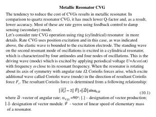
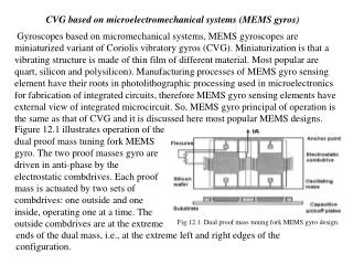
CVG based on microelectromechanical systems (MEMS gyros) Gyroscopes based on micromechanical systems, MEMS gyroscopes are miniaturized variant of Coriolis vibratory gyros (CVG). Miniaturization is that a vibrating structure is made of thin film of different material. Most popular are quart, silicon and polysilicon). Manufacturing processes of MEMS gyro sensing element have their roots in photolithographic processing used in microelectronics for fabrication of integrated circuits, therefore MEMS gyro sensing elements have external view of integrated microcircuit. So, MEMS gyro principal of operation is the same as that of CVG and it is discussed here most popular MEMS designs. Figure 12.1 illustrates operation of the dual proof mass tuning fork MEMS gyro. The two proof masses gyro are driven in anti-phase by the electrostatic combdrives. Each proof mass is actuated by two sets of combdrives: one outside and one inside, operating one at a time. The outside combdrives are at the extreme Fig.12.1. Dual proof mass tuning fork MEMS gyro design. ends of the dual mass, i.e., at the extreme left and right edges of the configuration.
The inside combdrives are between the two proof masses. The combdrives produce electrostatic forces and therefore can only pull the masses; they cannot push it. Therefore, an actuation cycle consists of four parts. During part-1, when the actuation voltage is applied, the outside combdrives pull the proof masses toward themselves while simultaneously the flexures supporting the proof masses deform storing elastic energy.During part-2 of the actuation cycle, when the voltage on the outside combdrives is reduced, the flexures straighten and bring the proof masses to their original, neutral, positions. At this point, actuation voltage is applied to the inside combdrives and the proof masses are pulled toward the inside while the flexures deform away from their equilibrium positions; this is part-3 of the actuation cycle. During part-4, when the actuation voltage is reduced again, the flexures return the proof masses to their neutral positions. If the vibrating proof masses are subjected to an angular rate, Ω, Fig. 12.2, around the central axis of the two proof masses, the Coriolis force is appeared. The Coriolis force will cause one of the proof masses to raise out-of-plane away from the substrate while the other proof mass drop Fig.12.2. Operation of the tuning fork MEMS gyro. down toward the substrate. The capacitive plates usually located under each of the proof masses and on the substrate under the proof masses sense the out-of-plane
Combdrives Combdrives Folded spring 111 m 50 m 3 m 200 m 10 m Proof mass Fig.12.4. MEMS gyro detail photo. Fig.12.3. Tuning fork MEMS gyro photo. displacement as a change in voltage. As the Coriolis force is proportional to angular rate, the voltage is proportional to angular rate, as well.Fig.12.3 illustrates photo of the MEMS gyrosensor. The proof masses, and each proof mass is supported by four folded springs, one at each corner as shown in fig.12.4 which is magnified red square area in fig.12.3. MEMS gyrosensor with electronics is depicted in photo fig.12.5. Fig.12.5. MEMS gyro with electronics
MEMS gyroscopes manufacturing process Before discussion of MEMS structure manufacturing process let’s consider some basic processes which are used during MEMS manufacture. Lithography Lithography in MEMS context is typically the transfer of a pattern into a photosensitive material by selective exposure to a radiation source such as light. A photosensitive material is a material that experiences a change in its physical properties when exposed to a radiation source. If a photosensitive material is selectively exposed to radiation (e.g. by masking some of the radiation) the pattern of the radiation on the material is transferred to the material exposed, as the properties of the exposed and unexposed regions differ. This exposed region can then be removed or treated providing a mask for the underlying substrate. Photolithography is typically used with metal or other thin film deposition, wet and dry etching. Electron beam lithography Electron beam lithography (often abbreviated as e-beam lithography) is the practice of scanning a beam of electrons in a patterned fashion across a surface covered with a film (called the resist), ("exposing" the resist) and of selectively removing either exposed or non-exposed regions of the resist ("developing").
The purpose, as with photolithography, is to create very small structures in the resist that can subsequently be transferred to the substrate material, often by etching Ion beam lithography It is known that focused-ion-beam lithography has the capability of writing extremely fine lines (less than 50 nm line and space has been achieved) without proximity effect. However, because the writing field in ion-beam lithography is quite small, large area patterns must be created by stitching together the small fields.
Electron Beam Deposition Electron beam depositionis a form of physical vapor deposition in which a target anode is bombarded with an electron beam given off by a charged tungsten filament under high vacuum. The electron beam causes atoms from the target to transform into the gaseous phase. These atoms then precipitate into solid form, coating everything in the vacuum chamber (within line of sight) with a thin layer of the anode material. Fig.12.6. Electron beam deposition set-up
Reactive ion etching (RIE) In reactive ion etching (RIE), the substrate is placed inside a reactor, and several gases are introduced. Plasma is formed in the gas mixture using an RF power source, which breaks the gas molecules into ions. The ions accelerate towards, and react with, the surface of the material being etched, forming another gaseous material. This is known as the chemical part of reactive ion etching. There is also a physical part, which is similar to the sputtering deposition process. If the ions have high enough energy, they can knock atoms out of the material to be etched without a chemical reaction. It is a very complex task to develop dry etches processes that balance chemical and physical etching, since there are many parameters to adjust. By changing the balance it is possible to influence the anisotropy of the etching, since the chemical part is isotropic and the physical part highly anisotropic the combination can form sidewalls that have shapes from rounded to vertical. RIE can be deep (Deep RIE or deep reactive ion etching (DRIE)). Fig.12.7. Reactive ion etching process
Deep reactive ion etching Deep RIE (DRIE) is a special subclass of RIE that is growing in popularity. In this process, etch depths of hundreds of micrometers are achieved with almost vertical sidewalls. The primary technology is based on the so-called "Bosch process", named after the German company Robert Bosch, which filed the original patent, where two different gas compositions alternate in the reactor. Currently there are two variations of the DRIE. The first variation consists of three distinct steps while the second variation only consists of two steps. In the 1st Variation, the etch cycle is as follows: (i) SF6 isotropic etch; (ii) C4F8 passivation; (iii) SF6 anisoptropic etch for floor cleaning. In the 2nd variation, steps (i) and (iii) are combined. Fig.12.8. Deep reactive ion etching (DRIE) process
Silicon substrate Cr/Au Top silicon Oxide layer Photoresist Cr/Au Top silicon Oxide layer Silicon substrate PSG Silicon substrate Top silicon Oxide layer MEMS gyro manufacturing process MEMS gyro manufacturing process consists of the following 8 stages: 1. The wafer is coated with PSG (phosphosilicate glass) and annealed to dope the top silicon layer with phosphorus. PSG is removed afterwards. 2. A negative photoresist is patterned by exposure and then Cr/Au metallization layer is deposited using e-beam deposition. 3. The photoresist is lifted-off and the metal layer on top is also removed this way. The remaining metal parts define the first metallization layer.
Photoresist Silicon substrate Top silicon Cr/Au Oxide layer Protective layer Cr/Au Top silicon Silicon substrate Photoresist Top silicon Cr/Au Silicon substrate 4. A masking photoresist is coated on to the front side and patterned with exposure. Using this photoresist mask the top silicon layer is etched with DRIE up to oxide layer. Photoresist is removed afterwards. 5. A masking photoresist is coated on to the back side and patterned with exposureand front layer is coated with a protective layer. Using this photoresist mask the bulk silicon layer is etched with DRIE up to oxide layer. Photoresist is removed. 6. The protective layer is removed. After that the oxide layer is removed making the structures suspended.
Shadow mask Silicon substrate Top silicon Cr/Au 7. Silicon made shadow mask is bonded to the SOI wafer for the masking layer of final metallization. The metal is evaporated and through the holes and stick to the SOI wafer. This metallization is important for substrate contact. 8. MEMS sample final view. Photo of real MEMS gyro is depicted in fig.12.9. Fig.12.9.