Download
1 / 72
800 likes | 1.42k Views
אוניברסיטת בן-גוריון בנגב הפקולטה למדעי ההנדסה המחלקה להנדסת חשמל ומחשבים. Scanning Probe Microscope - SPM -. Present Rony Levin Email levinbr@ee.bgu.ac.il Course Nanotechnology Number 361-2-0826 Lecturer Dr. Ilan Shalish. Agenda. Terms Definition Motivation Historical Overview

E N D
אוניברסיטת בן-גוריון בנגב הפקולטה למדעי ההנדסה המחלקה להנדסת חשמל ומחשבים Scanning Probe Microscope- SPM - Present Rony Levin Email levinbr@ee.bgu.ac.il Course Nanotechnology Number 361-2-0826 Lecturer Dr. Ilan Shalish
levinbr@ee.bgu.ac.il Agenda • Terms Definition • Motivation • Historical Overview • SPM Overview • STM Overview • AFM Overview • SPM Software • Summary
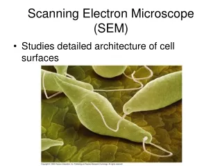
levinbr@ee.bgu.ac.il SurfaceDefinition • Surfaceis the shell of a macroscopic object (the inside) in contact with its environment (the outside world). An interface is the boundary between two phases. Object inside is called bulk • In large objects with small surface area A to volume V ratio (A/V) the physical and chemical properties are primarily defined by the bulk • In small objects with a large A/V-ratio the properties are strongly influenced by the surface
levinbr@ee.bgu.ac.il Lotus Leaf Phenomenon Hydrophobic effect Water Hydrophobic material Surface structure (20-100μm)
levinbr@ee.bgu.ac.il Semiconductor Devices Current flow near the surface In modern semiconductor devices surface is dominant
levinbr@ee.bgu.ac.il Semiconductor Production Layer by layer … Surface by surface…
levinbr@ee.bgu.ac.il Important Key Features of Surfaces • surface topography valley, planes, hills • physical materials behavior (conducting / insulating) • polarity (hydrophilic / hydrophobic) • tribological behavior (friction on "rough" or "smooth" surface) • physical surface behavior (reflectivity)
levinbr@ee.bgu.ac.il Application Examples of Surface Science • understanding and inhibition of corrosion • chip manufacturing / microelectronics • hard disks (anti-friction, ultra-smooth,...) • biological surfaces (patterned cell growth) • sensors (chemical, biological, electrical) • modification of anti-reflection (displays) • modification of wetting (inkjet printing)
levinbr@ee.bgu.ac.il Surface Research Motivation • According to all the mentioned before our motivation as electrical engineers for surface research is clear. The modern microelectronics devices properties, in general, affected by surface. • Moreover, we want not only passively receive information about the surface, but actively affect on it topology, moving the atoms
levinbr@ee.bgu.ac.il Terms Definition MicroscopyμΙκροσ - small, σκοποσ – see Scanning Probe Microscopy (SPM) is a branch of microscopy that forms images of surfaces using a physical probe that scans the specimen. SPM able to receive 3D surface topography
levinbr@ee.bgu.ac.il Terms Definition Local density of states (LDOS) is a physical space-resolved quantity that describes the number of states at each energy level that are available to be occupied. According to crystal's structure, this quantity can be predicted by computational methods, as for example with density functional theory Artifact is any perceived distortion or other data error caused by the instrument of observation
levinbr@ee.bgu.ac.il Terms Definition Input transducer or sensor Convert nonelectrical signal to electrical one Output transducer or actuator Convert electrical signal to nonelectrical one Piezoceramic Ceramic that convert electrical field to mechanical deformation and vice versa Piezoelectric properties are time-depended
levinbr@ee.bgu.ac.il Acronyms SPM Scanning Probe Microscope STM Scanning Tunneling Microscope AFM Atomic Force Microscope SFM Scanning Force Microscope FFM Force-Modulated AFM LFM Lateral Force Microscope MFM Magnetic Force Microscope SThM Scanning Thermal Microscope EFM Electrical Force Microscope
levinbr@ee.bgu.ac.il Historical Overview • 1981 STM was developed by Binnig and Rohrer, IBM, Zurich • 1986 AFM was developed by Binnig, Quarter and Gerber • 1988 Commercial SPM available • 1990 Analog electronics replaced by digital • 1990 Software for SPM based Microsoft Windows developed • from 1990 SPM market wake up Agilent Technologies, nanoScience …
levinbr@ee.bgu.ac.il SPM Physical ModelThe Blind Mouse Computer Actuator Probe Sample Sensor
levinbr@ee.bgu.ac.il Blind Mouse Operational Principle The blind mouse can’t see the object (sample), but using the stick (probe), he can scan it. Arm skin (sensor) send the received from the probe information to the brain (computer), the computer “see” the picture, if it need receive additional information about the sample (decision done using feedback), it send requirement to arm muscle (actuator), arm carefully moves the probe to required coordinate and vice versa
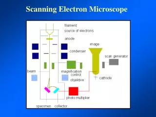
levinbr@ee.bgu.ac.il SPM Operational Principle All of the SPM techniques are based upon scanning a probe (typically called the tip, since it literally is a sharp metallic tip) just above a surface whilst between scanned surface and probe exist interaction The nature of this chosen interaction defines a device accessory to this or that type within the family of Scanning Probe Microscope The information on a surface is taken by fixing (by means of feedback system) or monitoring of interaction of a probe and the sample
levinbr@ee.bgu.ac.il SPM Operational Principle Surface divided to matrix of N rows by M columns Scanning performed row by row, as result we receive per each couple of coordinates {xi,yj}, vector with measurement results that described surface at this point
levinbr@ee.bgu.ac.il SPM Block Diagram
levinbr@ee.bgu.ac.il SPM Operational Principle We will present scanning probe microscopes based on two kind of iteration • Iteration is electrical currentSTM • Iteration is atomic forceAFM/SFM In general, as mentioned, SPM have two modes, defined by tip movement over the surface • Fixed probe Z coordinate, iteration or parameter depended on iteration monitoring • Fixed iteration, height change monitoring
levinbr@ee.bgu.ac.il STM Operational Principle Corral diameter ~ 14 nm Quantum Corral Tunneling current from site
levinbr@ee.bgu.ac.il STM Schematics
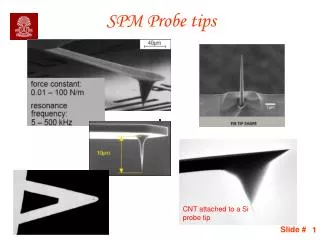
levinbr@ee.bgu.ac.il Probe Fabrication The tips are made simply by pulling the wires (typically 200 to 250 microns in diameter) using a pliers. A more consistent way to fabricate tips is using electrolysis. When the tip becomes very thin, it breaks living a very sharp tip appropriate to be used in the STM. The electrolytic bath is usually a solution of NaOH
levinbr@ee.bgu.ac.il Potential Barrier Schematics V is bias voltage EF is Fermi level
levinbr@ee.bgu.ac.il Step Potential Barrier Schrödinger time invariant equation
levinbr@ee.bgu.ac.il Transfer Matrix General solution Using C1 connectivity
levinbr@ee.bgu.ac.il Transfer Matrix Transfer Matrix Definition Now it can be written more simple
levinbr@ee.bgu.ac.il Transfer Matrix We received very powerful mathematical tool. Using this algorithm and Matlab we can solve complicated potential barriers
levinbr@ee.bgu.ac.il Rectangular Potential Barrier
levinbr@ee.bgu.ac.il Tunneling Probability
levinbr@ee.bgu.ac.il Tunneling - Summary Received result is not so suitable for classical physics theory, were electron position defined as “to be or not to be” In quantum mechanics theory electron position defined as “may be” and appropriate number from 0 to 1 that describe the chance of electron to be in some coordinate. Summarizing all the electrons over all energy levels, that can pass the barrier, will receive tunneling current expression
levinbr@ee.bgu.ac.il Tunneling Current
levinbr@ee.bgu.ac.il Distance Sensitivity What happened if current will be changed, how mach it will affect the distance? Assume that K=4 eV, current precision is 2%
levinbr@ee.bgu.ac.il STM Operational Mode • constant height mode: the tip is scanned over the surface keeping the vertical tip position constant, topography/conductivity differences are mapped by recording variations in tunnel current with respect to x−y−position of tip • constant current mode: the vertical tip position is adjusted during scanning to keep tunnel current constant, topography/conductivity map is constructed from vertical tip position with respect to x−y−position
levinbr@ee.bgu.ac.il LDOS Probing Using the current, STM probes the local density of states, and anything more Artifact, or another atom can create LDOS similar to atom, but STM can not distinguish it
levinbr@ee.bgu.ac.il What are We Imaging in STM? • Metals High density of states at atoms appear as bright protrusions • Insulators No conduction possible, we crash • Semiconductors and thin oxides Complex electronic structure at Fermi level , be careful!
levinbr@ee.bgu.ac.il Atom Manipulation Pulling modeThis mode uses the attractive forces between the tip and the adatom. The tip is positioned above the adatom and then brought towards the surface. The tunnel current increases. The tip is then moved horizontally. The current subsequently falls off until the adatom undertakes a hop towards the tip, while remaining on the surface. The current increases once more and the procedure continues
levinbr@ee.bgu.ac.il Atom Manipulation Pushing mode This is similar to the pulling mode except that it makes use of repulsive forces between the tip and the adatom. The tip is brought towards the surface and moved horizontally towards the atom. The latter jumps to the neighboring surface site. The current falls abruptly and the procedure continues
levinbr@ee.bgu.ac.il Atom Manipulation Sliding modeIn this mode the forces between the tip and the adatom are attractive, but the tip is so close to the surface that the adatom is attached onto it. As the tip approaches, the current increases and the adatom jumps onto the tip and remains there. When the tip moves horizontally parallel to the surface the current is related to the surface topography as seen by the tip with the attached adatom. Finally the tip is withdrawn and the adatom falls back onto the surface
levinbr@ee.bgu.ac.il Atom Manipulation Written literally with atoms, the Japanese Kanji, each just a few nanometers across - means “atom
levinbr@ee.bgu.ac.il STM Summary • STM is powerful technique for 3D viewing surfaces at the atomic level • STM require sample conductivity • STM can be used not only in vacuum, but also in air and various other liquid or gas ambient, and at temperatures range • STM allows manipulate atoms • STM probes the local density of states
levinbr@ee.bgu.ac.il STM – Catalog example
Laser Photo detector Cantilever levinbr@ee.bgu.ac.il AFM Operational Principle from site
levinbr@ee.bgu.ac.il AFM Schematics
levinbr@ee.bgu.ac.il Cantilever Cantilever is a beam supported on only one end
levinbr@ee.bgu.ac.il Cantilever
levinbr@ee.bgu.ac.il Cantilever Fabrication
levinbr@ee.bgu.ac.il Cantilever – Catalog example
levinbr@ee.bgu.ac.il Cantilever – Catalog example
levinbr@ee.bgu.ac.il Cantilever Regimes