Download
1 / 1
20 likes | 136 Views
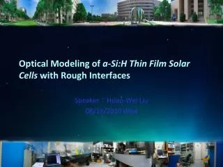
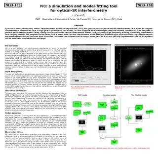
Φ FOR. P LOCAL. R j. R j+1. U=0. U=V. Φ REV. AZO L 1. Incident Light. x. x. x=j. x=j. x=j+1. x=j+1. a-Si L 2. AZO L 1 Z 1. a- Si:H L 2 Z 2. x. Z Input. 0. L. Reflection.

E N D
ΦFOR PLOCAL Rj Rj+1 U=0 U=V ΦREV AZO L1 Incident Light x x x=j x=j x=j+1 x=j+1 a-Si L2 AZO L1 Z1 a-Si:H L2 Z2 x ZInput 0 L Reflection • A New Design Tool for Nanoplasmonic Solar Cells using 3D Full Wave Optical Simulation with 1D Device Transport Models • Liming Ji* and Vasundara V. Varadan • Microwave& Optics Laboratory for Imaging & Characterization • University of Arkansas • * lxj001@uark.edu Plasmonic Layer L3 Ag Plasmonics L3 Z3 ZAg • Optimization of Nanoplasmonic Structure Designs • The dimension of each nanosplasmonic solar cell needs optimization to achieve the best performance for the solar cell. • Two challenges for optimization work: • 1) Numerical simulations are slow. Compared to the wavelength λg in each medium, the size of a thin film solar cell is usually > 5λg at 300 nm. Speed is a very important issue especially for finite element simulations. • 2) The optimization has to follow some guidelines. • The transmission line model and the concept of effective impedance can be used to describe a solar cell. Objective Integrate 3D full wave simulation with 1D carrier transport model to calculate the efficiency of nanoplasmonic solar cells. • 1D Carrier Transport Model • The AMPS 1D code is used for the numerical calculation of carrier transport in solar cells. • AMPS stands for Analysis of Microelectronic and Photonic Structures. • The computation of detailed carrier transport is done for the steady state of devices. • The device is divided into many small segments and the Poisson’s equation, as well as the continuity equations, are solved within each segment with the help of boundary conditions. • Introduction • The efficiency of nanoplasmonic solar cells is usually obtained through measurement of fabricated samples. • Fabricating a nanoplasmonic solar cell is expensive and time consuming. • Numerical simulations can quickly compute the efficiency of solar cells at low cost. • The available numerical codes for solar cells so far apply only to solar cells with all planar cells and they cannot account for: • 1) The particular distribution of absorbed power inside the semiconductor layer; • 2) The influence of the thickness of front and back passivation layers. Ψ is the electrostatic potential n & p are free electrons and holes density nt and pt are trapped electrons and holes ND+ and NA- are ionized dopings ε is the permittivity and q is the charge of an electron Poisson’s Equation The optimization of L1, L2 and Zinput will result in the best performance of a nanoplasmonic solar cell. Continuity Equation Gop is the optical generation rate R is the recombination rate Jn and Jp are electron and hole current densities Patterns of Localized Electric Field Light Absorption of A Solar cell with different Thickness of Front spacer Comparison between Transmission Line Calculation and Full Wave Simulation • From Full Wave Simulation to AMPS • The finite element High Frequency Structure Simulator (HFSS) is used for full wave simulations. • A 3D distribution of absorbed power inside the semiconductor is generated by HFSS and it is converted into a 1D pattern before exporting into the AMPS program. • The optical generation rate Gop in each small segment for electron-hole pairs are replaced by the imported 1D power distribution. • The J-V curve of the nanoplasmonic solar cell is calculated based on the imported Gop. • Methodology • The efficiency of nanoplasmonic solar cells can be calculated by integrating full wave simulations into the carrier transport model. • The key step is to obtain the optical generation rate of carriers in each nanoplasmonic solar cell. 1D Power Distribution in Si High 3D Power Distribution in Si Full Wave Simulation • Future Plan: 3D Carrier Transport Model • The accuracy can be improved if the 3D power distribution does not have to be converted into 1D distribution. • The optical generation rate and flow of carriers will have more directional details. • All derivative equations are three dimensional. Low Yes Optimization? Optmization of Nanoplasmonic Structure Comparison of the Original and New Methods for Gop Calculation Original Method New Method • Conclusions • The efficiency of nanoplasmonic solar cells can be calculated by combining the 1D carrier transport model with 3D full wave simulations • The optical generation rate of carriers is calculated based on the imported power distribution in the semiconductor. • The design of nanoplasmonic structure can be further improved by optimization using transmission line theory. • Developing the 3D carrier transport model can further improve the accuracy of the efficiency computation. No Obtain Power Distribution in Semiconductor Convert 3D Power Distribution into 1D Pattern Calculate Optical Generation Rate Export 1D Power Distribution into Carrier Transport Model Acknowledgement The authors acknowledge the research support provided by the National Science Foundation under EPS–1003970. The authors also thank Professor Stephen J. Fonash of the Pennsylvania State University for providing the source code of AMPS 1D. The carrier generation is calculated directly from the localized power density in each small segment. The carrier generation is dependent on the decreasing rate of the photon flows. ФFOR is the photon flow in the forward direction ФREV is the photon flow in the forward direction PLOCAL is the localized power density imported from HFSS Numerical Computation of Carrier Transport Optical Generation Rate Calculation Output Solar Cell Efficiency