Download
1 / 14
140 likes | 279 Views
1 CEA-DRT – LETI/DTS – CEA/GRE, Grenoble, France. 2 CEA-DSM – DRFMC – CEA/GRE, Grenoble, France. 3 IMEP, Grenoble, France. Towards the limits of conventionnal MOSFETs. G. BERTRAND 1 , S. DELEONIBUS 1 , B PREVITALI 1 , G. GUEGAN 1 , X. JEHL 2 , M. SANQUER 2 , F. BALESTRA 3. OUTLINE.

E N D
1CEA-DRT – LETI/DTS – CEA/GRE, Grenoble, France 2CEA-DSM – DRFMC – CEA/GRE, Grenoble, France 3 IMEP, Grenoble, France Towards the limits ofconventionnal MOSFETs G. BERTRAND1, S. DELEONIBUS1, B PREVITALI1,G. GUEGAN1, X. JEHL2, M. SANQUER2, F. BALESTRA3 ULIS 2003 Udine 20-21/03/03
OUTLINE • CMOS challenges • Device fabrication • Limits in terms of • Short Channel effects • Performances • Transport • Charge : from CMOS to SET-MOS • Conclusion ULIS 2003 Udine 20-21/03/03
CMOS challenges Possibilities of Conventional MOSFET? ULIS 2003 Udine 20-21/03/03
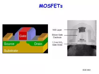
Device fabrication • Conventional MOSFET architecture- 1.2nm SiO2 gate oxide - In situ doped polysilicon Gate - Channel : non intentionnaly adjusted but Super Halo SH :(only BF2 halos) or Non super Halo NSH : (B II + BF2 halos) - As extensions - 30nm nitride spacers - As HDD Source and drain - RTP spike anneal 1050°C Gate length down to 16nm ULIS 2003 Udine 20-21/03/03
Limits : short channel effects (SCE) Electrical characteristics V =1.5V -3 10 d V =50mV d -5 10 Lot 6893 P18B • Field Effect transistor down to Lg=16nm Channel : B 5keV (A) 14 -2 LDD 1.5 10 cm -7 10 D I 13 -2 Halo 3.10 cm tilt 22° L = 29nm g -9 10 L = 16nm g -11 10 -0,5 0 0,5 1 1,5 W=10µm V (V) G ULIS 2003 Udine 20-21/03/03
Limits : short channel effects (2) • Below 40nm, SCE not efficiently controlled whatever transistor architecture: • spacer length (30 to 40nm) • halo dose (1-4.1013cm-2) • LDD dose (0.8-2.1014cm-2) Large punchtrough current below 40nm Need for : - Thinner gate oxide - Improvement of halo efficiency ULIS 2003 Udine 20-21/03/03
center channel doping - halo efficient doping- extension counter-doping : Rsd Limits : SCE (3) Halos efficiency Large B diffusion (TED+F) Halos : BF2 15-25keV ULIS 2003 Udine 20-21/03/03
Limits : Ion/Ioff High Rsd : Low IonOptimum SCE + Ioff control Medium Rsd : High IoffOptimum Ion • Despite large Rsd (~1200 .µm), Ion up to 900 µA/µm • OptimumRsd / SCE trade-off hard to perform with such conventionnal architecture and technique ULIS 2003 Udine 20-21/03/03
0,8 Vd=Vg=1.5V Lg=45nm Vd=1.5V Vg=1V 7 50 1,5 10 Lg=70nm 0,7 vsat 40 0,6 With Rsd correction 7 1 10 r velocity (cm/s) B (%) 0,5 30 LDD1 Lg=60nm Without Rsd correction 6 5 10 0,4 LDD 1 Lg=30nm LDD 2 Lg=60nm 20 LDD2 Lg=30nm 0,3 100 200 300 0 100 200 300 Temperature (K) Temperature (K) Degradation of low field mobility by halosoverlap and high transverse field operation due to Limits : transport (1) • No velocity overshoot • Quasi ballistic transport : r with T but r~0.5-0.6 whatever Lg < 100nm ULIS 2003 Udine 20-21/03/03
Limits : transport (2) • Impact at room temperature Low field mobility degradation due to halo overlapmostly in the case of efficient SCE control ULIS 2003 Udine 20-21/03/03
gate Small W Large W source drain D S D S G G island = channel SingleElectronTransistor(S.E.T.)Representation periodicoscillations SET Aperiodicoscillations Limits: from CMOS to SET-MOS (1) • Lg CMOS SET ULIS 2003 Udine 20-21/03/03
T=1.73K V =500µV L #30nm W=175nm d g Lot 8089 1E-9 1E-10 (A) d I 1E-11 1E-9 1,2 1E-12 0,4 0,6 0,8 1,0 1,2 1,4 1,6 V (V) g Limits: from CMOS to SET-MOS (2) > 50 oscillations @1.7K (0.5 to 1.4V) - Periodicity Related to Channel Geometry // F. Bœuf et al results [IEDM 2001]on non overlap Gate/Extension structure Importance of Rsd in Coulomboscillation observation ULIS 2003 Udine 20-21/03/03
-5 10 Lg=20nm W=10µm -6 10 Vd=100µV T=75K Vd=300µV -7 10 Vd=500µV Drain Current (A) -8 10 -9 10 T=20K -10 10 -11 10 -0,4 -0,2 0 0,2 0,4 0,6 Vg Limits: from CMOS to SET-MOS (3) • Observable oscillations from 20K up to 75K àminimal gate length àhigh charging energy • Aperiodic oscillations • Large W (10µm) • Enable SET- MOS operating temperature closer to room temperature if W is reduced ULIS 2003 Udine 20-21/03/03
Conclusions • Realization of conventional ultimate nMOSFET àfunctional devices physical gate length down to 16nm àelectrical characteristics with good performance • Limits :With conventional As extension + BF2 halos architecture : - difficult to control SCE below 40nm - limits low field mobility and non stationary transport Bulk : àNeed for thinner gate oxide (SCE control)àNeed for ultra steep halo profile (improved annealing process, B or In halo dopant instead of BF2, epitaxial SiCx diffusion barrier[VLSI 02]) Alternatives: low doped FDSOI, DGMOS. • From CMOS to SET-MOS - Conventional MOSFET could operate as SET at temperature below 4.2K - Promising results have been shown for 77K SET operation ULIS 2003 Udine 20-21/03/03