Download
1 / 35
360 likes | 571 Views
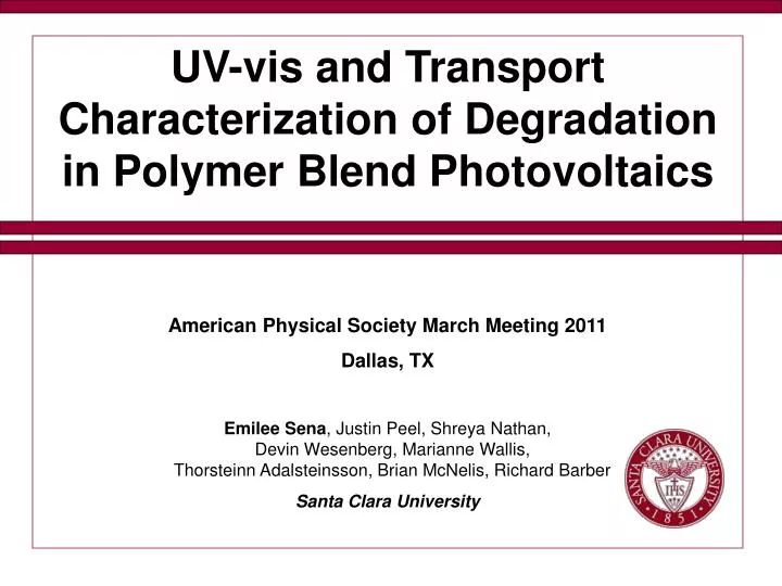
UV-vis and Transport Characterization of Degradation in Polymer Blend Photovoltaics American Physical Society March Meeting 2011 Dallas, TX Emilee Sena , Justin Peel, Shreya Nathan, Devin Wesenberg, Marianne Wallis, Thorsteinn Adalsteinsson, Brian McNelis, Richard Barber

E N D
UV-vis and Transport Characterization of Degradation in Polymer Blend Photovoltaics American Physical Society March Meeting 2011 Dallas, TX Emilee Sena, Justin Peel, Shreya Nathan, Devin Wesenberg, Marianne Wallis, Thorsteinn Adalsteinsson, Brian McNelis, Richard Barber Santa Clara University
Overview • Description of organic photovoltaics • How the devices work • Device fabrication • Device measurement • Active layer molecules • UV-vis spectroscopy
+ Charge Generator e- Charge Acceptor A - Multijunction What Are Organic Photovoltaic Devices? ħω A Multijunction Bulk Heterojunction
+ Charge Generator e- Charge Acceptor A A - Multijunction What Are Organic Photovoltaic Devices? ħω ħω ħω Bulk Heterojunction
+ Charge Generator e- Charge Acceptor A A - Multijunction What Are Organic Photovoltaic Devices? ħω ħω e- Bulk Heterojunction
+ Charge Generator e- Charge Acceptor A A - Multijunction What Are Organic Photovoltaic Devices? ħω ħω e- Bulk Heterojunction
+ Charge Generator e- Charge Acceptor A A - Multijunction What Are Organic Photovoltaic Devices? ħω ħω e- e- Bulk Heterojunction
Why Study Them? • Advantages over inorganic (silicon) solar cells: • Inexpensive • Flexible • Lightweight • Manufacturable • Why aren’t they used now?
Research Goals • Understandand improve • Device lifetime • Degradation • Power conversion efficiency
The Project • Physics: • Sample Fabrication • Measurement of Device Performance • Physical Chemistry: • Spectroscopic Analysis • Organic Chemistry: • Molecule Synthesis
How Are the Devices Made? • Indium-Tin-Oxide (ITO) • Indium-Tin-Oxide (ITO): “transparent” conductor (Cross section)
How Are the Devices Made? • Indium-Tin-Oxide (ITO) (Cross section)
How Are the Devices Made? • Indium-Tin-Oxide (ITO) • PEDOT:PSS • Indium-Tin-Oxide (ITO) • PEDOT:PSS PEDOT (poly(3,4-ethylenedioxythiophene)) PSS (poly(styrenesulfonate))
How Are the Devices Made? • Indium-Tin-Oxide (ITO) • PEDOT:PSS PEDOT (poly(3,4-ethylenedioxythiophene)) PSS (poly(styrenesulfonate))
How Are the Devices Made? • Indium-Tin-Oxide (ITO) • PEDOT:PSS • Active layer (or) P3HT (poly(3-hexylthiophene)) PCBOD ([6-6]-phenyl C61 butyric acid octadecyl ester) PCBM ([6-6]-phenyl C61 butyric acid methyl ester)
How Are the Devices Made? • Indium-Tin-Oxide (ITO) • PEDOT:PSS • Active layer • LiF
How Are the Devices Made? • Indium-Tin-Oxide (ITO) • PEDOT:PSS • Active layer • LiF • Al
How Are the Devices Measured? I recorded A V varied & recorded Solar simulator illuminates from below and I-V curves are generated
Device Performance Power Conversion Efficiency: ɳ = [(IV)max/area]/(Pin/area) Pin = 100 mW/cm2 |I*V|MAX (V,I)
The Active Layer • Electron donor and acceptor molecules • Light-induced electron transfer PCBOD + (or) P3HT PCBM
Meet the Molecules! • PCBM: [6,6]-phenyl-C61-butyric-acid-methyl-ester • PCBOD: [6,6]-phenyl-C61-butyric-acid- octadecyl-ester • Alkyl chain improves solubility, lifetime C60 PCBM PCBOD
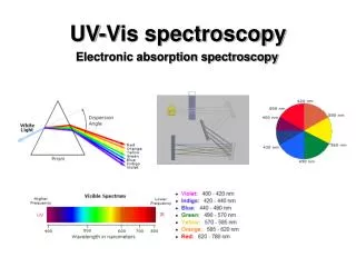
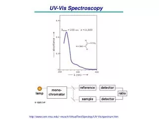
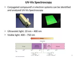
UV-Vis Spectroscopy: Why Do We Use It? • Insight into: • Absorption of light energy to excite electrons • Changes in chemical environment • Absorption changes due to degradation
750 nm 300 nm • How Does a Typical Spectrum Look? • Ultraviolet and visible range • Differential spectrum • Time evolution • MATLAB for analysis
Exponential Fit, Solve for Characteristic Time (τ): Ln [Amax – A (t) ] = -t / τ + constant Result for 554 nm: τ= 1/0.57 = 1.75 days IV data: τ= 1/0.56 = 1.79 days
Variable Factors • Weight percent • Blend stoichiometry • Annealing temperature • Most significant improvement in device performance
Annealing Anneal on hotplate (up to 380°C) (HEAT) Continue fabrication process with LiF and Al layers
Effects of Annealing: Device Performance 0.4 Molar Fraction PCBOD:P3HT Blend
0.16 Molar Fraction PCBM:P3HT Blend Not Annealed; PCEmax = 0.64 % Annealed at 220°C; PCEmax = 1.17% λmax = 555 nm Initial Spectrum Differential Spectrum 555 nm 450 nm
Effects of Annealing: Hypotheses • Decreased quenching • Morphological changes • Crystallite formation • Aggregation • More stable structure
Summary • Organic photovoltaics use light energy for electron transfer to produce current • UV-vis spectroscopy can be used to indicate changes in structure and chemical environment, how absorption changes with degradation • Annealing at high temperatures improves device performance
Funding • Santa Clara University's BIN-REU - UCSC BIN-RDI, NASA Grant NNX09AQ44A • SCU, Science Technology and Society Grants • Grant from IntelliVision Technologies Acknowledgements Michael Sena