Download
1 / 6
60 likes | 150 Views
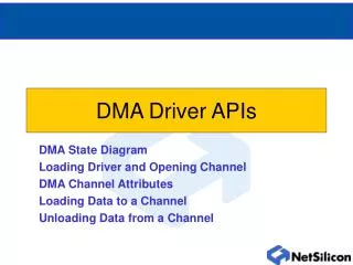
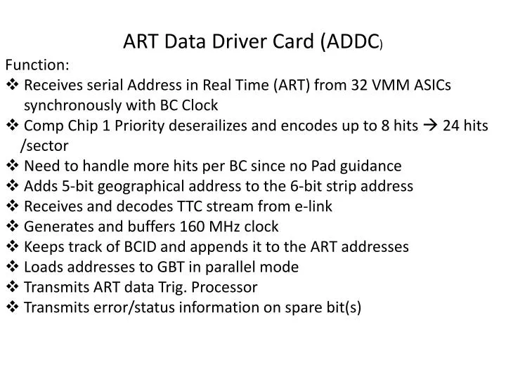
ART Data Driver Card (ADDC ) Function: Receives serial Address in Real Time (ART) from 32 VMM ASICs synchronously with BC Clock Comp Chip 1 Priority deserailizes and encodes up to 8 hits 24 hits /sector Need to handle more hits per BC since no Pad guidance

E N D
ART Data Driver Card (ADDC) • Function: • Receives serial Address in Real Time (ART) from 32 VMM ASICs • synchronously with BC Clock • Comp Chip 1 Priority deserailizes and encodes up to 8 hits 24 hits • /sector • Need to handle more hits per BC since no Pad guidance • Adds 5-bit geographical address to the 6-bit strip address • Receives and decodes TTC stream from e-link • Generates and buffers 160 MHz clock • Keeps track of BCID and appends it to the ART addresses • Loads addresses to GBT in parallel mode • Transmits ART data Trig. Processor • Transmits error/status information on spare bit(s)
De-serialize Hit Sel Data formatting
Issues, things to be decided • Use GBT + VTRx or GBT + VTT • Former uses down link for TTC and config but more expensive and doubles • fiber count • Latter uses much cheaper dual optical transmitters, does not require down • link fiber but requires two e-links for TTC and configuration • Geographical location of the 32 VMM chips • One plane • Pro: failure of link disables one plane • Con: Longer copper connections (~50 cm) • 4 layers by 8 VMM • Pro: Shorter connections (~20 cm) • Con: A track segment generates four hits limiting max independent hit it can • handle • ART Clock distribution • Common Clock per MMFE-8 • Pro: Only one multidrop LVDS line per MMFE-8 • Con: Requires skew adjustment, calibration/training (see Sorin’s talk) • One clock per VMM • Pro: automatic synchronization, no need for calibration • Con: More cables, weight, volume, power
Plans: • Design Prototype ADDC card • Possibly Use GBT samples and VTRx • If not available use GLIB • Use either prototype Comp.ASIC or implement in FPGA • Use with 4-layer chamber installed in CSC area of Wheel C • (2 needed) • Alternatively use one proto ADDC in test beam with 8 small MM • chambers • 60 GBT samples will be available next month (Moreiro talk last week) • Who/how many should we ask for? He warned that he expects demand to be high. No more than 2-3 to any given goup?