Download
1 / 3
30 likes | 186 Views
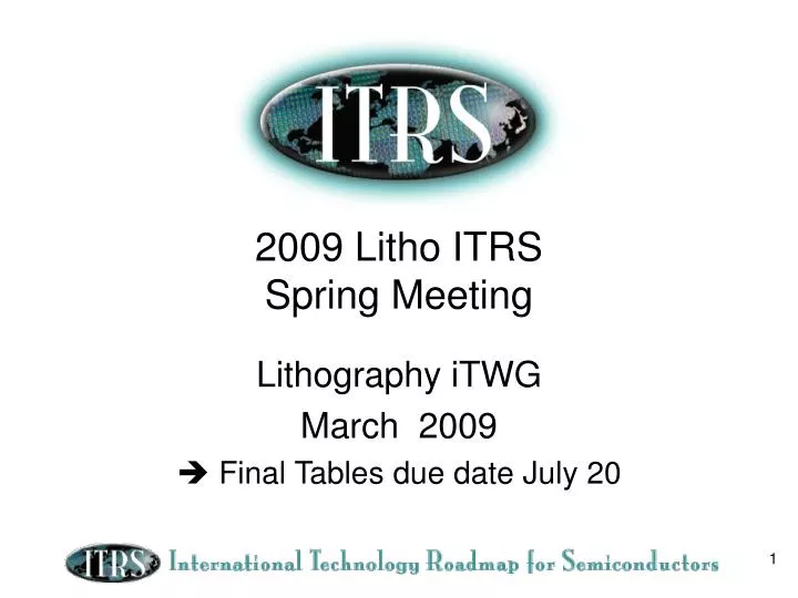
2009 Litho ITRS Spring Meeting. Lithography iTWG March 2009 Final Tables due date July 20. Lithography iTWG. Litho iTWG Technologies: Near/Long 193nm / EUVL / ML2, Imprint and Others Discussion EUVL@2013 (Near term 5 years 16nm ! ) “may be”

E N D
2009 Litho ITRS Spring Meeting Lithography iTWG March 2009 Final Tables due date July 20
Lithography iTWG • Litho iTWG • Technologies: Near/Long 193nm / EUVL / ML2, Imprint and Others • Discussion EUVL@2013 (Near term 5 years 16nm !) “may be” • EUVL Single Exposure Solution Advantage • “22nm” Table LITH1 “Various Techniques…” • 22nm Optical & 22nm EUVL * This table does not include the demands of Flash because it will be a less difficult Lithographic Process • Various Techniques for Achieving Desired CD Control and Overlay with Optical Projection Lithography for MPU and DRAM • Potential Solutions 2008 - 2009 update • Note – At 32 nm EUV only applies to MPU/DRAM; 193 DP/MP at 16nm only applies to Flash • 22nm EUV, 193 nm Immersion Double / Multiple Pattern, ML2, Imprint, • 16nm EUV, 193 nm Immersion Multiple Pattern, ML2, Imprint, Interference Lithography, DSA • 11nm EUV, ML2, Imprint, Interference Lithography, DSA • Tables: • MEEF on Mask CDU • LER/LWR Definition: (Gate/Wire/Contact via) Post development reduction & etch smoothing • Cross cut • ERM “More Photons” for scaling, MG function units bonding • Metrology Requirements from Litho TWG: *NGL/ML2 (+EUVL), • P/T 0.1, 0.2 discussion: Overlay capability 0.1, others 0.2, DP input from litho. TWG • Litho Requirements: Die-DB, Every wafer inspection • Yield Discuss: In-line Defect, Particle, EM, Haze/AMC • ESH: New material issues • M&S Near term,..