Download
1 / 18
290 likes | 914 Views
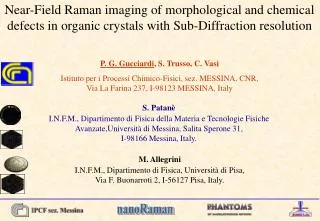
Sub-Diffraction Raman imaging by Near-Field Optical Microscopy. P. G. Gucciardi , S. Trusso, C. Vasi Istituto per i Processi Chimico-Fisici, sez. MESSINA, CNR, Via La Farina 237, I-98123 MESSINA, Italy. S. Patanè

E N D
Sub-Diffraction Raman imaging by Near-Field Optical Microscopy P. G. Gucciardi, S. Trusso, C. Vasi Istituto per i Processi Chimico-Fisici, sez. MESSINA, CNR, Via La Farina 237, I-98123 MESSINA, Italy S. Patanè I.N.F.M., Dipartimento di Fisica della Materia e Tecnologie Fisiche Avanzate,Università di Messina, Salita Sperone 31, I-98166 Messina, Italy. M. Allegrini I.N.F.M., Dipartimento di Fisica, Università di Pisa, Via Buonarroti 2, I-56127 Pisa, Italy.
High spatial resolution: 100 nm. Added value: simultaneous sample topography and elastic scattering images. Exploitation of Surface enhancement effects New Physics: Gradient-Field Raman Effect. Low efficiency of the Raman scattering. Low throughput of the SNOM Fiber probes. Very long acquisition times for Imaging purposes. High mechanical and thermal stability are required. Abstract Motivations: Difficulties: • Investigated Samples: • Tetracyanoquinodimethane (TCNQ) crystal showing surface defects. • Localized Cu-TCNQ complexes embedded in a TCNQ thin film.
Far-Field Vs Near-Field Microscopy Far-Field Microscopy Near-Field Microscopy • Both the light source and the antenna are placed at several wavelengths from the sample. • The Lateral resolution is determined by the Abbediffraction limit. • The sample is illuminated by a nanoscopic light source located close to the surface (10 nm). • The resolution is limited by the source diameter
Schematic of the Experiment • The sample is raster scanned by means of a piezo-tube under the probe. • SNOM probes: commercial single mode optical fibers, tapered and coated by a thin CrAl film. • The apical aperture is ~ 100 nm • Non-optical shear-force detection is accomplished for probe/sample distance stabilization, by means of a quartz tuning-fork.
Experimental setup • Excitation: Ar++ laser line 514.5 nm. • Collection: Nikon 50X objective, NA 0.5, WD 10.6 mm. • Notch Filter: Rejection Ratio ~ 10-6. • Spectrometer: Triax 190, single grating, 1200 lines/mm, 190 mm focal. • Detector: PMT in photon counting regime, 200-300 dark cts/sec. • Shear-Force: tuning-fork with etherodyne detection. • Signals: Topography, Elastic, Raman. • Modes: Illumination or Collection.
TCNQ 7,7’,8,8’ Tetracyanoquino-dimethane (TCNQ). • High Raman Efficiency. • The organometallic salt complexes can be discriminated based on the Raman shift of the vibrational peaks. • Can be deposited in thin film form or as a monocrystal. C-H Bending 1202 cm-1 CN Stretch 2225 cm -1 2208 cm -1 C=C ring Stretch 1620 cm-1 C=C wing Stretch:1445 cm -1 1380 cm -1
NanoRaman imaging of defects in TCNQ crystals • Surface defects are visible in the topography map. Topography • Both the micro and nano Raman analysis evidence a corresponding scattering incerase. • The nanoRaman map shows sub-diffraction length details. NanoRaman @ 1445 cm-1 MicroRaman @ 1445 cm-1
Another sample: a CuTCNQ thin film • A thin TCNQ film (yellow) was deposited on a KBr substrate in vacuum conditions. • The sample was kept into contact with Cu powders giving rise to localized spots of Cu-TCNQ (blue) organometallic compounds. • Areas in which the film is scratched out evidence the presence of the substrate (white). MicroRaman Spectra Optical Microphotograph TCNQ Scratch Cu-TCNQ
Our Target: Localization of: • TCNQ. • CuTCNQ Local spots. • Scratches evidencing the KBr substrate. On different length scales: Contrast mechanism: • Millimeter Microphotograph. • Micrometer MicroRaman. • Nanometer SNOM. Absorption Raman Activity Both
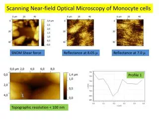
Localization of damaged areas by SNOM Localization by Reflectivity Topography Reflectivity • Scratched areas can be localized through the analysis of the surface topography. • The elastic scattering signal is locally enhanced because of the higher reflectivity of the KBr substrate. Localization by Raman Scattering Topography Raman @ 1445 cm-1 • Two holes appear in the topography. • A vanishing Raman activity is found therein. • Lateral resolution: ~ 300 nm.
Topography Elastic Scattering Topography shows no features NO SCRATCHES. Localization of CuTCNQ by SNOM The stronger absorption of the CuTCNQ is evident in the elastic scattering map. • Only 100 ms of integration time are required to get a Raman spectrum of TCNQ. • The CuTCNQ shows a Raman activity strongly reduced. Integration time 5 s. The Raman map at 1445 cm-1 (Tint= 100 ms per point) shows the presence of areas of depleted intensities which can be attributed to CuTCNQ. Raman Spectra Raman Map @ 1445 cm-1
Sub-diffraction Raman Imaging RAMAN Map @1445 cm -1 Raman Map Elastic Scattering • Integration time: 100 ms per point. Total image acquisition time: ~ 1 hour. • The zoom was carried out in the TCNQ zone. • The dark clusters can be attributed to the presence of CuTCNQ complexes localized on sub-micron length scales. • The line profile allows to assess a lateral resolution better than 200 nm.
CuTCNQ TOPOGRAPHY A different locations shows bump-like features. Scan width: 10 × 10 m2 The bumps turn out to be TCNQ-rich zones.
Resolution assessment in NanoRaman on Cu-TCNQ TOPOGRAPHY ELASTIC SCATTERING RAMAN 1445 cm -1 • Scan width: 2.5 × 2.5 m2 • Simultaneous maps of topography, Elastic and Raman scattering show correlated features. • Raman imaging confirms the spectral information on the chemical nature of the bumps. • A resolution of 240 nm can be assessed.
Difficulties in Illumination-mode SNOM NanoRaman experiments Metal-Phosphorus trichalcogenides NanoRaman TCNQ NanoRaman Spectrum • Raman emission of the SNOM fiber probe in the 100 – 500 cm-1 region. • High efficiency materials are “a must”. • Limited Spectral Resolution: 25 cm-1 • Image acquisition times of ~ 1h • Variations of the baseline.
… during the last year: • A very sensitive, versatile and performant SNOM setup was developed for spectroscopy applications. • NanoRaman imaging has been demonstrated on organic materials, within reasonable acquisition times. • Sub-diffraction resolution has been achieved. • Topography, Elastic and Raman scattering signals can be acquired simultaneously. • Critical points and limits of illumination mode Near-Field Raman experiments have been identified. • A class of materials suitable for NanoRaman investigations has been identified.
What’s next ? • Materials: Calchogenides, Nanotubes, Silicon. • Tecnhiques: SERS. • Instrumentation: Apertureless SNOM, Transmission mode, Different collection angles. • Upgrades: Better spectral resolution (5 cm-1), better spatial (10 nm) resolutions.
The New Concept • Different Probes: • Aperture SNOM • Scattering SNOM • AFM, STM • Olympus Microscope: • Localization • Light Collection • Micrometer screws: • Coarse positioning Thanks for the kind attention ! • Clearence: • Transmission Mode