Download
1 / 4
40 likes | 332 Views
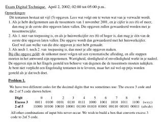
Clearly, F = XY + XZ + XYZ, and G = XZ + YZ. Clk. 1. Given the following two Boolean functions: F = (X + Y)(X + Z)(X + Y + Z), and G = (X + Z)(Y + Z). Init. CTR 4. CTR 4. Load Count D 0 Q 0 D 1 Q 1 D 2 Q 2 D 3 Q 3 CO. Load Count

E N D
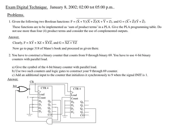
Clearly, F = XY + XZ + XYZ, and G = XZ + YZ Clk 1. Given the following two Boolean functions: F = (X + Y)(X + Z)(X + Y + Z), and G = (X + Z)(Y + Z). Init CTR 4 CTR 4 Load Count D0 Q0 D1 Q1 D2 Q2 D3 Q3 CO Load Count D0 Q0 D1 Q1 D2 Q2 D3 Q3 CO 1 Exam Digital Technique. January 8, 2002; 02:00 tot 05:00 p.m.. Problems. These functions are to be implemented as ‘sum of product terms’ in a PLA. Give the PLA programming table. Do not use more than four (4) product terms and consider the use of complemented outputs. Answer. Now go to page 318 of Mano’s book and proceeed as given there. 2. You have to construct a binary counter that counts from 9 through binary 69. You have to use 4-bit binary counters with parallel load. a) Give the symbol of the 4-bit binary counter with parallel load. b) Use two such counters and logic gates to construct your 9 through 69 counter. c) Add an additional input to the counter that initializes it synchronously to 9 when the signal INIT is 1. Answer.
Answer. Format: XY/Z (x = unspecified) Present state Input Next state Output A X Y A Z 0 0 0 0 0 0 0 1 0 x 0 1 0 1 1 0 1 1 0 x 1 0 0 1 0 1 0 1 0 x 1 1 0 1 0 1 1 1 0 x 10/1 x0/0 x1/x 00/0 x1/x 3. A serial leading 1’s detector is to be designed. A binary integer of arbitrary length is presented to the serial leading 1’s detector most significant bit first on input X. When a given bit is presented on input X, the corresponding output bit is to appear during the same clock cycle on output Z. Z = 0 as long as the bits applied to X are zero. When the first 1 is applied to X, Z=1. For all bit values applied to X after the first 1 is applied, Z=0. To indicate that a sequence is complete and that the circuit is to be initialized to receive another sequence, input Y becomes 1 for one clock cycle. Otherwise Y=0. a) Find the state diagram for the serial leading 1’s detector. b) Find the state table for the serial leading 1’s detector.
4. Find an algorithmic state machine (ASM) chart for a traffic light controller that works as follows: A timing signal T is the input to the controller. T defines the yellow light interval, as well as the changes of the red and green lights. The outputs to the signals are defined by the following table: Output Light Controlled GN Green Light, North/South Signal YN Yellow Light, North/South Signal RN Red Light, North/South Signal GE Green Light, East/West Signal YE Yellow Light, East/West Signal RE Red Light, East/West Signal S0 S1 S2 S3 GN RE YN RE RN GE RN YE While T=0, the green light is on for one signal and the red light for the other. With T=1, the yellow light is on for the signal that was previously green, and the signal that was previously red remains red. When T becomes 0, the signal that was previously yellow becomes red, and the signal that was prevoiusly red becomes green. This pattern of alternating changes in color continous. Assume that the controller is synchronous with a clock that changes much more frequently than input T. 0 1 1 0 0 1 1 0 T T T T Answer.
5. Logic to implement transfers among three registers R0, R1, and R2 is to be designed. The register transfers are as follows: CA : R1R2, R0R2 CB : R1R0 CC : R0R1, R2R0 The control variables are mutually exlcusive; i.e., only one variable can be equal to 1 at any time, while the other two are equal to zero. You have to use one multiplexer-based bus and one direct connection from one register to another. a) Find the register transfer table below: Operation Select Load Answer. Operation Select Load R0 L0 L1 L2 0 S1 S2 1 2 S1 S2 3-to-1 mux CA: R1R2, R0R2 1 0 1 1 0 CB: R1R0 0 0 0 1 0 CC:R0R1, R2R0 0 1 1 0 1 L0 R1 CC S0 CC L2 CA S1 CA CA CC CB L1 R2 L0 L1 Clk L2 b) Find simple logic that converts the control variables to the select inputs of the multiplexer and the load inputs of the registers. c) Draw a detailed logic diagram of the hardware implementing a single bit of this register transfers.