Download
1 / 22
220 likes | 360 Views
High performance field programmable gate array for gigahertz applications. Jong-Ru Guo, C. You, M. Chu, K. Zhou, Jin-Woo Kim, B.S. Goda*, R.P. Kraft, J.F. McDonald Rensselaer Polytechnic Institute, Troy, NY, 12180 * United State Military Academy, West Point, N.Y. 10096. Gigahertz era.

E N D
High performance field programmable gate array for gigahertz applications Jong-Ru Guo, C. You, M. Chu, K. Zhou, Jin-Woo Kim, B.S. Goda*, R.P. Kraft, J.F. McDonald Rensselaer Polytechnic Institute, Troy, NY, 12180 * United State Military Academy, West Point, N.Y. 10096
Gigahertz era High speed reconfigurable system is needed to handle the increasing amount of data. However, the CMOS FPGA just is operated at the hundreds MHz. GHz reconfigurable system is needed.
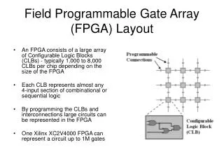
IntroductionField Programmable Gate Array (FPGA) B FPGA: A reconfigurable chip that can be programmed for a specific function. Status: There are no FPGA’s that operate at GHz microprocessor clock rates much less at K-band or X-band. Goal: Change this situation for the better. A C I/O Cell Routing Cell Logic Cell K-band: 10.9~36GHz X-band: 8-12GHz
FPGA Applications • Prototyping • Digital Networks • - Mobile Subscriber Equipment • - High Speed Switching Nodes • 2. Real Time Signal/Image Processing • - Radar • - Pattern Recognition • 3. Digital System Processing • - Filters • - Fourier Transform • 4. Satellite Systems • 5. Wireless
High speed IBM SiGe HBT Process Approximated cut-off frequency: IBM 0.5 & 0.25 um generations (5HP) ~ 50 GHz IBM 0.18 um generation (7HP) ~ 120 GHz IBM 0.13 um generation (8HP) ~ 180 GHz 8HP process 7HP process 5HP process Observe the Logarithmic Ic Axis Ref. 40-Gb/s Circuits Built From a 120-GHz fT SiGe Technology IEEE Journal of Solid-State Circuit. VOL. 37, NO.9, Sept. 2003
Eg,Ge(x=0) Drift Field p-SiGe base e- EC n+ Si emitter h+ EV n- Si collector Ge (Concentration) Eg,Ge(x=0) Eg,Ge(grade)= Eg,Ge(x=Wb)- p-Si x SiGe Graded Base Bipolar Transistor Ref. Flash Comm Si/SiGe band diagram Ref. Yuan Taur and Tak H. Ning “Fundamentals of Modern VLSI Devices”, Cambridge University Press, p364, 1998.
Input 17:1 MUX West Output MUX Input 16:1 MUX Input 17:1 MUX 2:1 MUX North Output MUX East Output MUX South Output MUX Output drivers Memory configuration structure Master-Slave Latch New Structure: Input and Output Block and Function Unit (FU) Ce,Qe,E,E4 Cw,Qw,W,W4 Cs,Qs,S,S4 Cn,Qn,N,N4 E,S,N To East Ce,Qe,E,E4 Cw,Qw,W,W4 Cs,Qs,S,S4 Cn,Qn,N,N4 W,S,N To West C Ce,Qe,E,E4 Cw,Qw,W,W4 Cs,Qs,S,S4 Cn,Qn,N,N4 Q E,W,S To South New D-FF CLK E,W,N To North Function Unit (FU) Input Routing block Output routing block Schematic of the new function unit Based on XC6200 (170um x 210um)
170 um 210 um Area improvement-BC 130 um 135 um 49% layout area saved 7HP: 0.18 um process 8HP: 0.13 um process Smaller layout Better performance More Configurable cells.
Prediction of the performance improvement by the different generation processes 130 ps 100 ps 42 ps 30 ps??? 71 mW 52 mW 13.8 mW 4.2 mW 5HP 7HP 8T 9HP? HBT Generations Propagation delay and power consumption comparisons between different processes
Test circuit Four stage Basic Cell ring oscillator-BC Measurement result of the 7HP ring oscillator Measurement result of the 5HP Basic Cell
Power-saving scheme- Basic Cell Power-saving scheme Usage [12] Case I: Only combinational logic or sequential logic is used. Case II: Sequential logic and redirection function are used. Case III: Only redirection function is used.
Layout size has been reduced by 49%. With the latest Basic Cell, there will be 48x48 Basic Cell array in 7mm x 7mm area. Propagation delay has been reduced by 82.5% Power consumption has been reduced by 80.6% (5HP case and 8HP power saving case) for the fully turned-on case. There is 94% power saved when the power-saving scheme is enabled. Summary: Basic Cell
Interleaving block Interleaving data path High speed inputs High speed front end De-interleaving data path SiGe FPGA CMOS FPGA To processors or other circuits High speed outputs High speed back end DSP and other applications Such as, Poly-phase filter, digital filter…etc De-interleaving block 100MHz~700MHz 500MHz ~ 10GHz 10GHz ~ 80GHz High speed reconfigurable system
Application: High speed data acquisition system MUX-DEMUX • SiGe FPGA can be configured to DSP and other applications. • To compare the performance between the SiGe and CMOS FPGAs, the SiGe FPGA is configured to be 4:1 MUX and 1:4 DEMUX. • The results can be used to prove its interleaving and de-interleaving functions.
D1 D1B CH1 CH1B D3 D3B CH2 CH2B Data Output OutputB D2 D2B CH3 CH3B 1:2 DEMUX D4 D4B CH4 CH4B ¼ CLK out CLK ½ DIV ½ DIV 1/2 CLK 1/2 CLKB CLK CLKB 1/2 DIV The block diagram of the 4:1 MUX The building blocks of the 1:4 DEMUX. Outputs CHx Output CH1 CH2 CH3 CH4 4T T 1:4 DEMUX input Data input CH1 CH3 CH2 CH4 CHx T 2:1 MUX 2:1 MUX 2:1 MUX 1:2 DEMUX 1:2 DEMUX 4T The timing diagram of the 4:1 MUX (x represents 1, 2, 3 and 4) The timing diagram of the 1:4 DEMUX High speed data acquisition MUX-DEMUX
Layout of the 4:1 MUX and 1:4 DEMUX implemented by the SiGe Basic Cells Simulation results show both 4:1 MUX and 1:4 DEMUX can operate up to 10GHz Compare to CMOS FPGA (Xilinx Virtex), same circuits can run to 183MHz Layout of the 4:1 MUX Layout of the 1:4 DEMUX
Simulation results (MUX) Simulation result of the 4:1 MUX. Inputs: CH_A: 1010011, CH_B: 0010100, CH_C: 0101001 and CH_D: 0001010. Output: 0010-1000-0011-1100-0001-0110. Simulated eye diagram of the 4:1 MUX programmed by SiGe FPGA runs at 10Gbps
SiGe and CMOS FPGAPerformance comparisons Virtex results are based on the following environments: Software: Foundation 2.1 Xilinx power consumption work sheet V1.5
Larger scale SiGe FPGA 5.8mm • 20x20 Basic Cell array is fabricated by IBM (7HP). with the dimension of 7mm x 7mm. (400 Basic Cells). • 48x48 Basic Cell array is developed (8HP) with the high speed ADC integrated. 7mm
The performance of the SiGe FPGA can reach up to 20GHz (8HP generation) The layout has been reduced by 49% between the 8HP and 5HP generations. Applications have been proposed to run at GHz range. 4:1 MUX and 1:4 DEMUX have been configured to compare the performance of SiGe and CMOS FPGA. Conclusion
Future work • Test 20x20 Basic Cell array has been fabricated by IBM (7HP). • Develop high speed data acquisition system. • Implement DSP applications. Such as software radar, poly phase filtering …etc. • 10GHz and 20GHz SiGe FPGA. • Integrated with high speed front-end and back-end circuits. Primitive layout of the 48x48 SiGe FPGA