Download
1 / 22
220 likes | 318 Views
EET 252 Unit 5 Programmable Logic: FPGAs & HDLs. Read Floyd, Sections 11-5 to 11-10. Study Unit 5 e-Lesson. Do Lab #5. Lab # 5a due next week. Homework #5 and Lab # 5b due in two weeks. Midterm exam next week. Review.

E N D
EET 252 Unit 5Programmable Logic: FPGAs & HDLs • Read Floyd, Sections 11-5 to 11-10. • Study Unit 5 e-Lesson. • Do Lab #5. • Lab #5a due next week. • Homework #5 and Lab #5b due in two weeks. • Midterm exam next week.
Review Programmable Logic Devices (PLDs) are ICs with a large number of gates and flip flops that can be configured to perform a specific logic function or perform the logic for a complex circuit. Major types of PLDs are: SPLD: (Simple PLDs) are the earliest type of array logic used for fixed functions and smaller circuits with a limited number of gates. (The PAL and GAL are both SPLDs). CPLD: (Complex PLDs) are multiple SPLDs arrays and inter-connection arrays on a single chip. FPGA:(Field Programmable Gate Array) are a more flexible arrangement than CPLDs, with much larger capacity.
Figure 11.34 The basic concept of an LUT programmed for a particular SOP output.
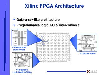
FPGAs An FPGA uses a different architecture than a CPLD. The configurable logic block (CLB) or logic array block (LAB) is the basic element which is replicated many times. CLBs are arranged in a row and column structure. Within the CLBs are logic modules joined by local interconnects. Generally, the logic modules are composed of a look-up table (LUT), a flip-flop, and a MUX that can be used to bypass the flip-flop for strictly combinational logic.
FPGAs Logic modules can be configured for combinational logic, registered logic, or a combination of both. The global interconnects distribute signals (including the clock) to various CLBs. FPGAs may also have a “hard core” portion of logic that is put in by the manufacturer and cannot be reprogrammed by the user. These FPGAs are useful in commonly used functions such as I/O interfaces.
FPGA Cores • Most SPLDs and CPLDs are completely blank when you buy them. • Because FPGAs are so dense, many chip-makers give the option of manufacturing some of the circuitry to perform a specific function, such as a microprocessor or a RAM. • Such pre-programmed circuitry is called a core.
Hard Core, Soft Core, IP • A hard core is a core that cannot be reprogrammed by the user. • A soft core is a core that the user can reprogram to some extent. • Cores are also referred to as intellectual property (IP), since the chip-maker retains ownership of the core design. • Example on Altera’s website.
Review: Programmable Logic Software All manufacturers of programmable logic provide software to support their products. The process is illustrated in the flowchart. The first step is to enter the logic design into a computer. It is done in one of two ways: 1) Schematic entry 2) Hardware description language (HDL).
Review: Programmable Logic Software In schematic entry, the design is drawn on a computer screen by placing components and connecting then with simulated wires. After drawing the schematic, it can be reduced to a single block symbol:
Programmable Logic Software In text entry, the design is entered via a hardware description language such as VHDL or Verilog.
Hardware Description Languages (HDLs) • Many hardware description languages (HDLs) exist for text entry of PLD designs. • Learning an HDL takes longer than learning to do schematic entry. But for complex designs it can provide a more powerful and simpler way to enter designs.
Some Popular HDLs • Open-standard HDLs • VHDL (IEEE 1076) • Verilog (IEEE 1364) • Proprietary HDLs • CUPL • ABEL (Advanced Boolean Expression Language, now owned by Xilinx) • AHDL (AlteraHDL)
A VHDL Sample One way of writing VHDL programs is to use Boolean-type statements. There are two parts to such a program: the entity and the architecture. The entity portion describes the I/O. The architecture portion describes the logic. Following is a short VHDLprogram showing the two parts. entityExample is port (B,C,D: in bit; X: out bit); endentityExample; architecture Behavior of Example is begin X <= (B or C) and D; endarchitectureBehavior;
A Verilog Sample Another standard HDL is Verilog. In Verilog, the I/O and the logic is described in one unit called a module. Verilog uses specific symbols to stand for the Boolean logical operators. The following is the same program as in the previous slide, written for Verilog: moduleExample (X, B, C, D); input B, C, D; output X; assign X = (B | C)&D; endmodule
Boundary Scan Logic Boundary scanlogic is circuitry on a PLD whose purpose is to let users test and program the chip. The JTAG standard (IEEE 1149.1) is a widely used open standard that defines four internal registers and five I/O signals for this purpose. Under normal operation, the boundary scan logic is “invisible”.
JTAG (IEEE 1149.1) Registers and I/O Signals • Registers • Boundary scan register • Bypass register • Instruction register • Optional: Identification register • I/O Signals • TDI (Test Data In) • TDO (Test Data Out) • TMS (Test Mode Select) • TCK (Test Clock) • Optional: TRST (Test Reset) • See pp. 4-5 of Altera UP1 Board manual (on course website).
Figure 11.62 Greatly simplified diagram of a JTAG compliant (IEEE Std. 1149.1) programmable logic device (CPLD or FPGA). The BSCs (boundary scan cells) form the boundary scan register. Only a small number of BSCs are shown for illustration.
Selected Key Terms A type of one-time programmable SPLD that consists of a programmable array of AND gates that connects to a fixed array of OR gates. PAL GAL Macrocell CPLD A reprogrammable type of SPLD that that is similar to a PAL except it uses a reprogrammable process technology, such as EEPROM instead of fuses. Part of a PAL, GAL, or CPLD that generally consists of one OR gate and some associated output logic. A complex reprogrammable logic device that consists basically of multiple SPLD arrays with programmable interconnections.
Selected Key Terms FPGA Design flow Schematic entry Text entry Boundary scan Field programmable gate array; a programmable logic device that uses the LUT as the basic logic element and generally employs either the antifuse or SRAM-based process technology The process or sequence carried out to program a target device. A method of placing a logic design into software using schematic symbols. A method of placing a logic design into software using a hardware description language (HDL). A method for internally testing a PLD based on the JTAG standard (IEEE Std. 1149.1).