Download
1 / 45
450 likes | 569 Views
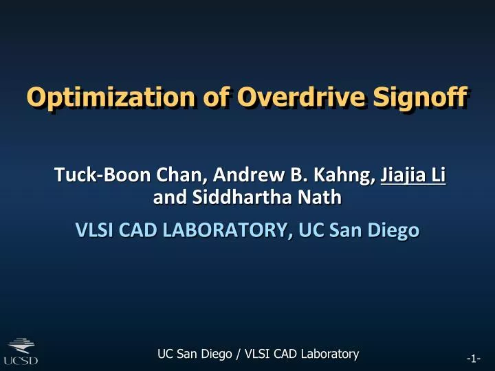
Optimization of Overdrive Signoff . Tuck-Boon Chan, Andrew B. Kahng, Jiajia Li and Siddhartha Nath VLSI CAD LABORATORY, UC San Diego. Outline. Motivation Design Cone Dominance of Modes Problems and Methodologies Experimental Setup and Results Conclusions and Ongoing Works. Outline.

E N D
Optimization of Overdrive Signoff Tuck-Boon Chan, Andrew B. Kahng, Jiajia Liand Siddhartha Nath VLSI CAD LABORATORY, UC San Diego
Outline • Motivation • Design Cone • Dominance of Modes • Problems and Methodologies • Experimental Setup and Results • Conclusions and Ongoing Works
Outline • Motivation • Design Cone • Dominance of Modes • Problems and Methodologies • Experimental Setup and Results • Conclusions and Ongoing Works
Motivation Vdd • Mode = (voltage, frequency) pair • Multi-mode operation requires multi-mode signoff • Example: nominal mode and overdrive mode • Selection of signoff modes affects area, power • Our Goal: Optimally select signoff modes • Improve performance, power, or area • Reduce overdesign OD OD NOM NOM time tnom tOD tnom tOD
Fix Nominal Mode Overdrive Frequencies (MHz) 1000 90 - 92 mW > 95 mW • The average power of circuits signed off with different overdrive modes • Average power = r x POD + (1-r) x Pnom • r is the duty cycle of overdrive mode 950 93 - 95 mW 87 - 89 mW 90 - 92 mW 900 < 87 mW 850 93 - 95 mW 800 1.03 1.05 1.07 1.09 1.11 1.13 1.15 1.17 Overdrive Voltages (V) fnom = 500MHz Vnom= 0.9V Different overdrive modes 20% power range
Fix Nominal Mode + OD Frequency • Power of circuits signed off with different overdrive voltages • Low signoff voltage large # of buffers • High signoff voltage high dynamic power 14% fnom = 500MHz Vnom= 0.9V fOD = 950MHz
Outline • Motivation • Design Cone • Dominance of Modes • Problems and Methodologies • Experimental Setup and Results • Conclusions and Ongoing Works
Tradeoff between Frequency & Voltage • Voltage scaling frequency vs. voltage tradeoff curves • Maximum frequency increases essentially linearly with supply voltage • We approximate such curves as straight lines
Design Space for Signoff • Design space for signoff is the set of all possible combinations of signoff modes • Example: design space for two-mode signoff is all combinations of two points in the plane Frequency Circuit (frequency vs. voltage tradeoff) curve Mode (voltage, frequency) Voltage
Design Cone • Design cone is theunion of all the feasible operating modes (frequency, voltage pairs) for circuits signed off at one mode • Determined by tradeoff between frequency and voltage (slopes of frequency vs. voltage tradeoffs) • Indicates the solution space for signoff mode selection Frequency The design cone of mode A A Voltage
Estimation of Design Cone • Slope of frequency vs. voltage tradeoff (MHz/V) mainly determined by threshold voltages • Gate type, fanouthave little influence • Wire resistance also has little influence • 10,000X change in resistance <2% change in slopes
Estimation of Design Cone • Slope of frequency vs. voltage tradeoff (MHz/V) mainly determined by threshold voltages • Gate type, fanouthave little influence • Wire resistance also has little influence • 10,000X change in resistance <2% change in slopes
Estimation of Design Cone • Slope of frequency vs. voltage tradeoff (MHz/V) mainly determined by threshold voltages • Gate type, fanouthave little influence • Wire resistance also has little influence • 10,000X change in resistance <2% change in slopes
Estimation of Design Cone • Slope of frequency vs. voltage tradeoff (MHz/V) mainly determined by threshold voltages • Gate type, fanouthave little influence • Wire resistance also has little influence • 10,000X change in resistance <2% change in slopes
Estimation of Design Cone • Slope of frequency vs. voltage tradeoff (MHz/V) mainly determined by threshold voltages • Gate type, fanouthave little influence • Wire resistance also has little influence • 10,000X change in resistance <2% change in slopes
Estimation of Design Cone • Slope of frequency vs. voltage tradeoff (MHz/V) mainly determined by threshold voltages We use inverter chains with LVT- and HVT-only cells to estimate the boundary of design cone
Outline • Motivation • Design Cone • Dominance of Modes • Problems and Methodologies • Experimental Setup and Results • Conclusions and Ongoing Works
Dominance • One mode is outside of the design cone of the other positive / negative timing slacks Frequency Negative Slack Design Cone of mode A HVT • Above the design cone Negative timing slacks • Below the design cone Positive timing slacks C LVT A B Positive Slack Voltage
Dominance • One mode is outside of the design cone of the other positive / negative timing slacks • M2 shows positive timing slacks w.r.t. M1 M1 is the dominant mode Frequency Design Cone of mode A HVT • Mode A is the dominant mode LVT A B Voltage
Dominance • One mode is outside of the design cone of the other positive / negative timing slacks • M2 shows positive timing slacks w.r.t. M1 M1 is the dominant mode • Positive timing slacks indicate overdesign Frequency Design Cone of mode A HVT • Mode A is the dominant mode • Shift mode B to B’ • reduce voltage and power • retain same performance LVT A B’ B Positive Slack Voltage
Equivalent Dominance • When two modes exhibit equivalent dominance • No one is dominated by the other • They are in each other’s design cone Frequency B Mode A and B exhibit equivalent dominance A Voltage Multi-mode signoff at modes which do not exhibit equivalent dominance leads to overdesign
Outline • Motivation • Design Cone • Dominance of Modes • Problems and Methodologies • Experimental Setup and Results • Conclusions and Ongoing Works
The 3+1 Problems • Overdrive signoff has four parameters • Nominal mode: , • Overdrive mode: , fnom Vnom fOD VOD • Given fnom, fOD and Vnom, search for VOD • Given fnom, fOD and VOD, search for Vnom Minimize power • Given Vnom, VOD and fnom, search for fOD • Given Vnom, VOD and fOD, search for fnom Maximize performance under power constraints
The 2+2 Problems • Overdrive signoff needs four parameters • Nominal mode: fnom, Vnom • Overdrive mode: fOD, VOD • FIND_OD: given (fnom, Vnom), search for (fOD, VOD) maximize fODs.t. average and peak power satisfy constraints • FIND_VOLT: given fnom and fOD, search for Vnom and VOD minimize average power
Reduction from 2+2 to 3+1 • 2+2 problems can reduce to 3+1 problems by sweeping one unknown parameter 3+1 Problem Solver 3+1 Problem Solver fnom fnom fnom fnom • Reduction of FIND_OD problem VOD_1, VOD_2, ... fOD_1, fOD_2, ... fOD Vnom Maximum fOD MiminumPavg fOD fOD Vnom Vnom VOD VOD Corresponding Vnom Corresponding VOD Sweep VOD Sweep Vnom Vnom_{1, 2,...} VOD_{1, 2,...} • Reduction of FIND_VOLT problem
Methodologies for 3+1 Problems • Given fnom, fOD and Vnom, search for VOD • Given fnom, fOD and VOD, search for Vnom Minimize power Exhaustive search on the solution space defined by given parameters and design cone Frequency Frequency Overdrive Mode fOD fOD Solution space fnom fnom Nominal Mode Vnom VOD Voltage Voltage
Methodologies for 3+1 Problems • Given Vnom, VOD and fnom, search for fOD • Given Vnom, VOD and fOD, search for fnom Maximize performance under power constraints Scale frequency along the solution space until the power constraint is hit Frequency Frequency Overdrive Mode fOD Solution space Nominal Mode fnom Vnom VOD Vnom VOD Voltage Voltage
Common Design Practice Today: Signoff & Scale (FIND_OD) • Sign off circuit at nominal mode • Scale the voltage to increase frequency until the power constraint is hit • Simplifies the design process, but ignores second (OD) mode in the signoff Frequency Overdrive Mode fOD fnom Nominal Mode Vnom VOD Voltage
Proposed Flow (FIND_OD) • Signoff & scale at nominal mode to estimate the maximum overdrive frequency (fest) Frequency fest fnom Nominal Mode Vnom Voltage
Proposed Flow (FIND_OD) • Signoff & scale at nominal mode to estimate the maximum overdrive frequency (fest) • Determine several approximate overdrive modes based on fest and the design cone Frequency fest Approximate overdrive modes fnom Nominal Mode Vnom Voltage
Proposed Flow (FIND_OD) • Signoff & scale at nominal mode to estimate the maximum overdrive frequency (fest) • Determine several approximate overdrive modes based on fest and the design cone • Implement voltage scaling on each approximate overdrive mode until hit the power constraint Frequency Overdrive Mode (highest fOD) fest fnom Nominal Mode Vnom Voltage
Proposed Flow (FIND_VOLT) • Exhaustive search for Vnom minimum power at nominal mode Nominal power Voltage Frequency fOD fnom Vnom Voltage
Proposed Flow (FIND_VOLT) • Exhaustive search for Vnom minimum power at nominal mode • Estimate the design cone of selected mode Voltage Frequency fOD fnom Vnom Voltage
Proposed Flow (FIND_VOLT) • Exhaustive search for Vnom minimum power at nominal mode • Estimate the design cone of selected mode • Exhaustive search for VOD within the design cone minimum average power Voltage Frequency fOD fnom Vnom VOD Voltage
Outline • Motivation • Design Cone • Dominance of Modes • Problems and Methodologies • Experimental Setup and Results • Conclusions and Ongoing Works
Experimental Setup • Design: AES (~15K instances) from OpenCores • Technology: TSMC65nm • Comparison • Signoff&Scaleapplies traditional signoff and scale methodology • Proposed implements our proposed flow • Exhaustive Search uses exhaustive search
Experimental Results (FIND_OD) • Proposed flow improves performance by 7% • Flow requires about 22% runtime compared to exhaustive search with similar area (-0.01%), power (+3%) and performance (-0.5%) Nominal mode: fnom= 500MHz Vnom = 0.9V
Experimental Results (FIND_VOLT) • Flow requires about 27% runtime compared to exhaustive search with similar area (-0.01%), power (+8%) fnom = 500MHz / fOD = 600MHz Signoff & Scale is not applicable to FIND_VOLT
Recent Updates • Problem: too many SP&R runs • Approach: • Use power models for global optimization • Avoid implementing circuits at each mode • Construct power model adaptively • Small constant # runs is enough scalable
Global Optimization Flow • Iteratively sample and refine the power models Sample (SP&R) Circuit information Construct power models Power models Estimate optimal signoff modes Estimated optimal mode Sample (SP&R) Circuit information Refine power models
Example • Performance of the proposed global optimization 1.20V 0.90V 1.10V 1.08V 1.06V Frequency = 800MHz , Voltage = ?
Outline • Motivation • Design Cone • Dominance of Modes • Problems and Methodologies • Experimental Setup and Results • Conclusions and Ongoing Works
Conclusions & Ongoing Works • Conclusions • Study the problem of signoff mode selection • Propose the concept of design cone • Show that mutual equivalent dominance is required for signoff mode selection to avoid overdesign • Propose methodologies for signoff mode selection • Ongoing Works • More accurate estimation of design cone • Consider additional tradeoffs of design metrics such as area, reliability
Acknowledgments • Work supported by IMPACT, SRC, NSF, Qualcomm and Samsung