Download
1 / 4
50 likes | 221 Views
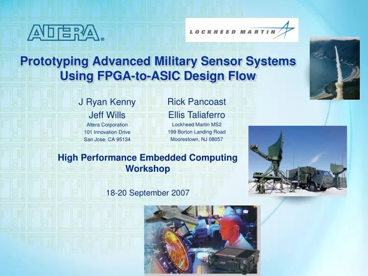
Prototyping Advanced Military Sensor Systems Using FPGA-to-ASIC Design Flow. Rick Pancoast Ellis Taliaferro Lockheed Martin MS2 199 Borton Landing Road Moorestown, NJ 08057. High Performance Embedded Computing Workshop 18-20 September 2007. J Ryan Kenny Jeff Wills Altera Corporation

E N D
Prototyping Advanced Military Sensor Systems Using FPGA-to-ASIC Design Flow Rick Pancoast Ellis Taliaferro Lockheed Martin MS2 199 Borton Landing Road Moorestown, NJ 08057 High Performance Embedded Computing Workshop 18-20 September 2007 J Ryan Kenny Jeff Wills Altera Corporation 101 Innovation Drive San Jose, CA 95134
HardCopy II PhysicalOptimization Design FPGA to HardCopy ASIC Device Design Flow Approve Design? Target HardCopy II Device Customer Handoff to HardCopy Design Center Validate Design In-System With Stratix II FPGA Sensor Prototype Sensor Production
Hard Copy ASIC Device – What Why • True Structured ASIC • Only Top Layers Custom • FPGA Architecture with ASIC Routing • Flexibility of FPGA Design with Cost and SWaP Features of ASIC • Reduce: • Power by 50-70% (over FPGA) • Design time from 52 Weeks (ASIC) to 20 Weeks (Hard Copy) • Unit Cost after NRE estimated of $350,000 • Risk – virtually zero risk conversion • Size by 60-85% • Can be same pinout • Up to 50% Performance Improvement
Compute Node (Notional Architecture) Power: 3 FPGA = 60 Watts Memory\Other = 40 Watts DC-to-DC Loss = 20 Watts I\O (Serial) = 80 Watts FPGA FPGA FPGA FPGA Compute Node (200 Watts) Create Smaller Module HC HC Create Hard Copy Drop-In Chips HC HC HC HC Reduce Power by 80 Watts (40%) Reduce Power by 40 Watts (20%)