Download
1 / 31
330 likes | 519 Views
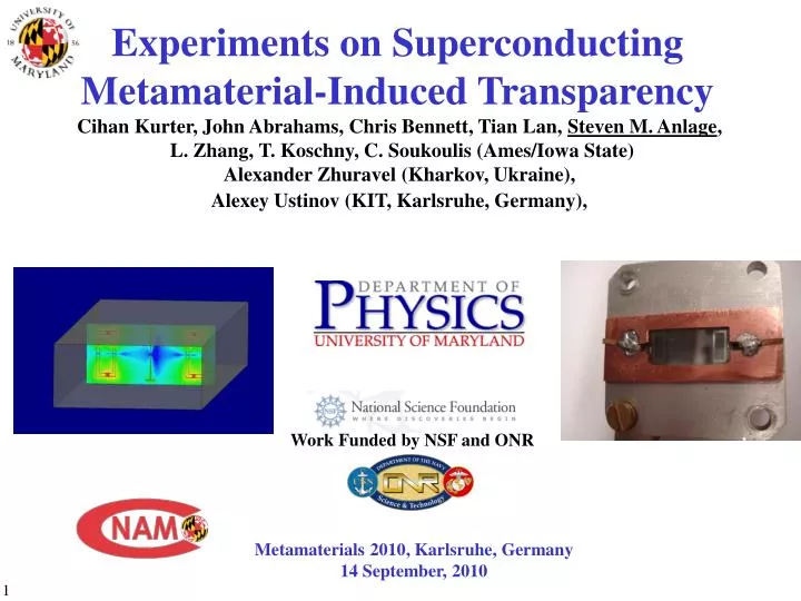
Experiments on Superconducting Metamaterial-Induced Transparency Cihan Kurter, John Abrahams, Chris Bennett, Tian Lan, Steven M. Anlage , L. Zhang, T. Koschny, C. Soukoulis (Ames/Iowa State) Alexander Zhuravel (Kharkov, Ukraine), Alexey Ustinov (KIT, Karlsruhe, Germany),.

E N D
Experiments on Superconducting Metamaterial-Induced Transparency Cihan Kurter, John Abrahams, Chris Bennett, Tian Lan, Steven M. Anlage, L. Zhang, T. Koschny, C. Soukoulis (Ames/Iowa State) Alexander Zhuravel (Kharkov, Ukraine), Alexey Ustinov (KIT, Karlsruhe, Germany), Work Funded by NSF and ONR Metamaterials 2010, Karlsruhe, Germany 14 September, 2010
Metamaterial-Induced Transparency Inspired by: Electromagnetically-Induced Transparency (EIT) Strong dispersion with little loss Probe Absorption Probe Frequency Probe Frequency Probe Field N. Papasimakis, et al. Optics and Photonics News, Oct. 2009 Pump Field Classical Analog of EIT Garrido Alzar, et al., Am J Phys (2002) Atom g1 g2 Dissipation g2 << g1 to coherently drive particle 1 Light can be slowed, or even stopped at the EIT frequency L. V. Hau, Nature (1999) Fleischhauer, PRL (2000)
Classical Analog of EIT The Importance of Strong Loss Contrast The “atom” has zero displacement at the EIT frequency, but large displacement for small de-tuning Atom Re[x1(t)] g2 g1 Pump Field Probe Field g2 << g1 g1 = 4.0 x 10⁻² g2 = 1.0 x 10⁻⁷ Absorbed Power
Metamaterial-Induced Transparency Work with L. Zhang, T. Koschny, and C. Soukoulis (Iowa State Univ.) Normal metal metamaterials: Papasimakis, PRL 2008 Tassin, PRL 2009 Superconducting Metamaterials MIT @ 10 GHz Nb Nb Cu X-band waveguide E Cu (radiative) Normal metal B Nb (dark) Superconducting g1 g2
Simulation Results Metamaterial-Induced Transparency L. Zhang, T. Koschny, and C. Soukoulis (Iowa State Univ.) Transmission and Reflection Index of Refraction EIT Frequency Adjust coupling to dark resonators and frequencies of dark resonators to modify n(w) dispersion
Experimental Setup Metamaterial-Induced Transparency Network Analyzer 1 2 Coaxial Cable Cryogenic Dewar X-band Waveguide Sample
Superconductor Electrodynamics T = 0 ideal s-wave s1(w) s2(w) ~ 1/w s = s1-is2 ns(T) Normal State (T > Tc) (Drude Model) sn s2(w) s1(T) T 0 (p nse2/m)d(w) Tc 0 s1(w) T 0 Tc 0 Superfluid density l2 ~ m/ns w 0 1/t 0 “binding energy” of Cooper pair (100 GHz ~ few THz) Surface Impedance (w > 0) Superconducting State (w < 2D) Normal State Penetration depth l(0) ~ 20 – 200 nm Finite-temperature: Xs(T) = wL = wm0l(T) → ∞ as T →Tc Narrow wire or thin film of thickness t : L(T) = m0l(T) coth(t/l(T)) → m0l2(T)/t Kinetic Inductance
Experimental Results Metamaterial-Induced Transparency Pin = -30 dBm T = 4.6 K Nb / Cu MM-EIT sample (first generation) in Cu waveguide EIT bandwidth (3 dB) = 7.5 MHz (~ 0.1%)
Superconducting Metamaterial-Induced Transparency Effect of Temperature on Transmission 0 -5 -10 Transmission |S21|/|S21|max (dB) -15 -20 -25 Frequency (GHz)
Superconducting Metamaterial-Induced Transparency Effect of Temperature on Group Delay Pin = -30 dBm
Experimental Results Metamaterial-Induced Transparency Switching/Limiting Behavior at High Power The “transparency window” switches off between +17 and +18 dBm
RF Power Dependence of Superconducting EIT Features To investigate the RF power dependence, we examine the RF current distributions in the superconducting parts of the sample using Laser Scanning Microscopy (LSM) See A. P. Zhuravel, et al., J. Appl. Phys. 108, 033920 (2010)
LSM Image of Superconducting RF Currents in EIT sample @ 10 GHz 2D LSM image Geometry Focus on this corner Nb split ring Upper Nb split ring f = 9.63 GHz; P = 18 dBm; T = 7 K Cu stripe Bottom Current flow numerical simulation, L. Zhang, et al. (Ames) C. Kurter, et al., arXiv:1008.2020
RF Power Dependence of LSM Photoresponse in a Corner of the Nb Split Ring Nb film 100 mm Quartz substrate 100 mm 15 dBm 20 dBm 20.6 dBm 20.8 dBm 21 dBm 22 dBm
Future Directions for Superconducting EIT Metamaterials Rounded-corner samples for better tunability at high power Calibrated and de-embedded S21 and group delay measurements
Conclusions Demonstrated Superconducting Metamaterial-Induced Transparency Tunable with variable Kinetic Inductance and RF magnetic fields Demonstrated Tunability of EIT features: Temperature tuning (kinetic inductance → plasmonic regime) RF Magnetic Field tuning (magnetic Abrikosov vortices, JRF peaks) Superconducting Metamaterials Review Article (J. of Optics, in press): arXiv:1004.3226 Work Funded by NSF, ONR.
CryoCoolers and CryoPackaging Small, inexpensive and reliable cryocoolers are available Stirling cycle cryocooler MTBF > 106 hours +compressor! 2.8 kg 92 mm OD x 300 mm 5W cooling power @ 77 K Many companies build cryo-cooled microwave and high-speed digital products STI “AmpLink” Filter 1850 – 1910 MHz PCS band
Outline Losses in Metamaterials Brief Review of Superconductor Electrodynamics New Features Enabled by Superconductivity Low loss (+ inductance) enables very compact ‘atoms’ New sources of inductance New sources of nonlinearity and gain New ‘Atoms’ Some Novel Applications of Superconducting Metamaterials Future Prospects + Conclusions Review article on Superconducting Metamaterials (J. of Optics) arXiv:1004.3226
Flat Lens Imaging Cloaking Devices (Engheta, Leonhardt, Pendry, Milton) RHM RHM LHM Point source “perfect image” Why Superconducting Metamaterials? The exciting novel applications of metamaterials: Flat-slab Imaging “Perfect” Imaging Cloaking Devices Illusion Optics etc. … Illusion Optics (Lai) … have strict REQUIREMENTS on the metamaterials: Low Losses Ultra-small size “atoms” (size << wavelength) Tunability / Texturing of the index of refraction n SUPERCONDUCTING METAMATERIALS: Can achieve these requirements!
Outline Losses in Metamaterials Brief Review of Superconductor Electrodynamics New Features Enabled by Superconductivity Low loss (+ inductance) enables very compact ‘atoms’ New sources of inductance New sources of nonlinearity and gain New ‘Atoms’ Some Novel Applications of Superconducting Metamaterials Future Prospects + Conclusions
sn s1(T) T 0 Tc 0
g2 = 1 x 10⁻² g2 = 1 x 10⁻³ Absorption g1 = 4 x 10⁻² g2 = 1 x 10⁻⁷ Frequency
Experimental Results Metamaterial-Induced Transparency This includes transmission losses in cold cables and waveguide Nb / Cu MM-EIT sample (first generation) in Cu waveguide
Experimental Results Metamaterial-Induced Transparency Switching/Limiting Behavior at High Power |S21| (dB) The “transparency window” switches off between +17 and +18 dBm Frequency (GHz)
Laser Scanning Microscopy of RF Currents Principle of the Measurement Work with A. Zhuravel (Kharkov) and A. Ustinov (Karlsruhe) modulated laser resonator transmission laser OFF Pout |S21(f0)|2 Pin laser ON |S21(f0)|2 f f0 co-planar resonator f0 ~ 5.2 GHz D|S12|2 ~ [lJRF(x,y)]2 A dl Local heating produces a change in transmission coefficient proportional to the local value of JRF2 J. C. Culbertson, et al. J.Appl.Phys. 84, 2768 (1998) A. P. Zhuravel, et al., Appl.Phys.Lett. 81, 4979 (2002)
2-D Response Map for RF Current Distribution of a Sample Fundamental resonance mode (5.2 GHz) 8.5 mm 1 mm 10 mV RF photoresponse ~ Jrf2(x, y) LAO 0 mV T = 79.5 K f = 5.2133 GHz P = - 6 dBm 240 nm thick film
Standing Wave JRF Pattern at Fundamental Frequency T=79.5 K with 8672 A Generator P=-6 dBm in scale of 8672A Fmod=99.99 kHz f=5.2133 GHz Photoresponse (a.u.) Fit: 2D image kfit = 0.39 mm-1 ktheory = 0.42 mm-1 Proof that measured PR ~ JRF2 to first order approx.