Download
1 / 9
790 likes | 3.79k Views
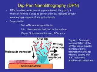
Dip-Pen Nanolithography (DPN). DPN is a direct-write scanning-probe-based lithography in which an AFM tip is used to deliver chemical reagents directly to nanoscopic regions of a target substrate Components: Pen: AFM scanning cantilever

E N D
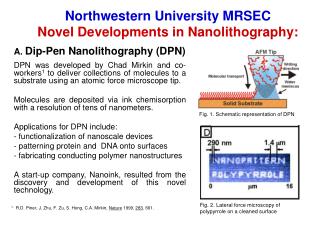
Dip-Pen Nanolithography (DPN) • DPN is a direct-write scanning-probe-based lithography in which an AFM tip is used to deliver chemical reagents directly to nanoscopic regions of a target substrate • Components: Pen: AFM scanning cantilever Ink: the materials that bind to the surface Paper: Substrate such as Au, SiOx, mica Figure 1. Schematic representation of the DPN process. A water meniscus forms between the AFM tip which is coated with “ink” molecules and the solid substrate
Direct-Write DNP procedure • Prepare the ink (Fe2O3nanoparticles hydrosol) • Prepare the paper (mica & silicon, surface treatment by aqueous HF solution) • Coat the cantilever with the ink • Scan the area for patterning in the contact mode, with a slower scan rate, 1 µm s-1 • For AFM characterization, use the same AFM, scan it at higher scan rate, 10 µm s-1
Direct-Write DNP for protein array • Prepare the ink (MHA: mercaptohexadecanoic acid) • The paper (silicon slides) • Coat the cantilever with the ink • Scan the area for patterning in the contact mode. • Protein adsorption (rabbit IgG ) • antibody recognition. • The resulting protein arrays were then characterized by AFM. B) Topography image of the protein array
Direct-Write DNP for protein array Height profiles of TM-AFM images: rabbit IgG assembled on an MHA dot array generated by DPN before (A) and after (B) treatment with a solution containing lysozyme, goat/sheep anti-IgG, human anti-IgG, and rabbit anti-IgG; a control protein nanoarray before (C) and after (D) exposure to a solution containing lysozyme, retronectin, goat/sheep anti-IgG, and human anti-IgG.
Nanostructures patterned by DPN • Nanoscale dot arrays and B) nanoscale letters written on a Au surface • C) TM-AFM image of 25- and 13-nm gold nanoparticles hybridized to surface DNA templates generated with DPN D) Fluorescence image of DPN patterns • of fluorescently labeled IgG on SiOx
Nanostructures patterned by DPN B) TM-AFM image of 60-nm gold nanolines C)12-nm gold nanogap on a Si/SiOx surface. D) 3D Si(100) nanostructures. TM-AFM image of DNA-modified line (E), features after hybridization with complementary DNA-modified nanoparticles; insert: high-resolution TM-AFM images
Advantages It might be the only lithographic technique that offers • High resolution • High registration • With direct-write printing capabilities
Limitation of the method More efforts should be put in improving the speed and in transforming it into massively parallel process to be a powerful production tool in both the life science and the semiconductor industry.
Conclusions • DPN is a unique scanning-probe-based lithographic tool for generating high-resolution patterns of chemical functionality on a nano range of surfaces. • The combination of resolution, registration, and direct-write capability offered by DPN distinguishes it from any alternative lithographic strategy and makes DPN a promising tool for patterning soft organic and biological nanostructures.