Download
1 / 15
150 likes | 260 Views
Recent studies on a single-walled carbon nanotube transistor. Reference : (1) Mixing at 50GHz using a single-walled carbon nanotube transistor, S.Rosenblatt, et al, Appl. Phys. Lett. 87, 153111 (2005).

E N D
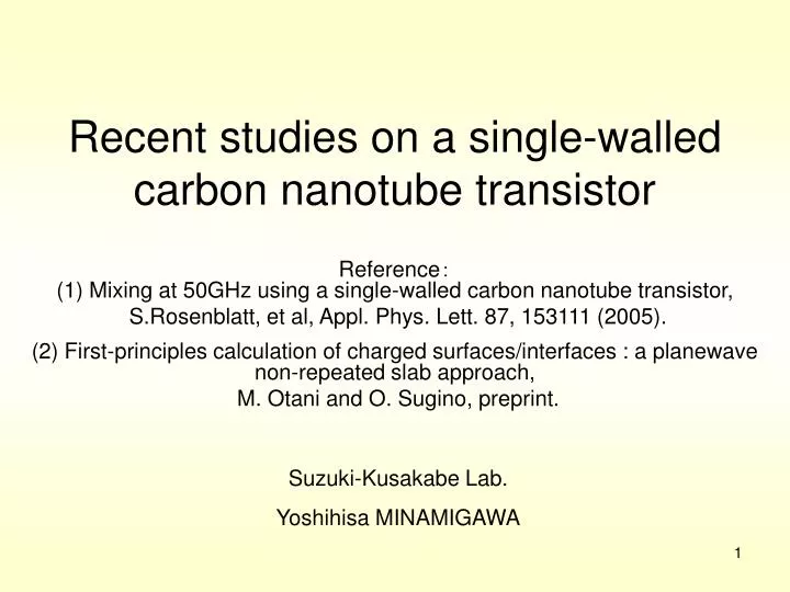
Recent studies on a single-walled carbon nanotube transistor Reference:(1) Mixing at 50GHz using a single-walled carbon nanotube transistor, S.Rosenblatt, et al, Appl. Phys. Lett. 87, 153111 (2005). (2) First-principles calculation of charged surfaces/interfaces : a planewave non-repeated slab approach, M. Otani and O. Sugino, preprint. Suzuki-Kusakabe Lab. Yoshihisa MINAMIGAWA
Contents • Introduction • background knowledge of CNT-FET • Experimental results – Reference 1 • Novel calculation technique - Reference 2 • Results of calculation • Summary CNT-FET : Carbon nanotube Field effect transistor
Introduction : CNT-FET • Reason that SWNT is used in FET • High charge mobility • Nano size structure · diameter : 1~few nano meters · length : ~1µm 1) 1) Nano letter. Vol.4 No.1 35-29 (2004)
CNT Electric field Gate Introduction : CNT-FET • Air gap structure • Field effect dope Air gap It is our goal to elucidate physics of a CNT of such a condition theoretically.
Nanotube in a condenser + = +++ +++ ++++ ++++ Electrostatic Potential - - - - - - = + Nanotube in a FET = + ? Electrostatic Potential ? = + Introduction : Difficulty of first principle calculation of CNT-FET Unit cell Unit cell
Experiment : CNT-FET Mixer circuit Nanotube Contact layer : 50nm thick Pd Gate : 2 μm width Al Source and Drain : Au , Au-Pd alloy Source-Drain contact gap : 3 μm HR-Si : High resistively Si
(1) The peak in correlates with the position of the peak in . + : :Experimental data ∘ : :Model data from Eq.(1) Experimental results – Reference 1
(1) Experimental results – Reference 1
When Source-drain bias is enough small, conductance can be provided by Greenwood-Kubo formula from wave function or charge density. Relation of experiment and calculation If under various is calculated, we expect that will enable theoretic analyses of CNT-FET.
Novel calculation technique - Reference 2 • Main techniques of First principle calculation • APW (Augmented plane wave) method • KKR (Korringa-Kohn-Rostoker) method • Pseudo potential method • Real space method APW, KKR and Pseudo potential method has credibility and much know-how. But, these are only used under a periodic boundary condition. Real space method don’t need a periodic boundary condition. But, Know-how of this method is not enough.
We can do high precision simulating “CNT-FET”. Novel calculation technique - Reference 2 • This novel technique’s character is… • Using Pseudo Potential method • Periodic boundary condition is not necessary in one direction. • To place “a virtual electrode” is possible.
(2) : Electrostatic potential : Green function : Total electron charge density (3) : relative permittivity Novel calculation technique - Reference 2 Eq(2) and Eq(3) are solution of Poisson equation under a condition that x and y direction is uniformity.
Until now Novel technique d: 6.34Å 16.3Å Gate CNT Gate Gate CNT 16.3Å 10.1Å x Unit cell y Unit cell z Condition of calculation The same structure repeat to direction of x and y axis. The same structure repeat to direction of x, y and z axis.
Electrode Semi-conducting tube Results of calculation Electric field near nanotubes
Summary • We can calculate the state of CNT which charge doped by the field effect. • To calculate conductance G in a state of nearly zero bias( ). Next work