Download
1 / 21
210 likes | 253 Views
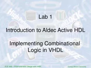
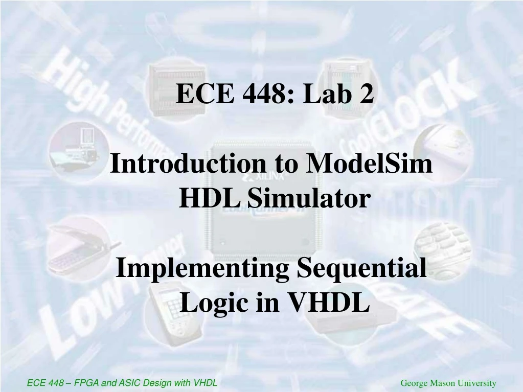
ECE 448: Lab 2 Introduction to ModelSim HDL Simulator Implementing Sequential Logic in VHDL. ECE 448 – FPGA and ASIC Design with VHDL. George Mason University. Introduction to ModelSim HDL Simulator. Example: MLU. MLU Block Diagram. 0 1. 0 1. 0 1. MUX_0. A1. A. MUX_4_1. Y1.

E N D
ECE 448: Lab 2 Introduction to ModelSim HDL Simulator Implementing Sequential Logic in VHDL ECE 448 – FPGA and ASIC Design with VHDL George Mason University
Introduction to ModelSim HDL Simulator Example: MLU
MLU Block Diagram 0 1 0 1 0 1 MUX_0 A1 A MUX_4_1 Y1 IN0 MUX_1 NEG_A IN1 MUX_2 Y OUTPUT IN2 SEL0 IN3 SEL1 NEG_Y B1 B L1 L0 MUX_3 NEG_B
Experiment 2 Part 1 Debouncing Circuit
Switch Key Bouncing key bounce, tBOUNCE key bounce, tBOUNCE typically, tBOUNCE < 10 ms
Key Debouncing key bounce, tBOUNCE key bounce, tBOUNCE typically, tBOUNCE < 10 ms debouncing period output = last input sampled = 0 debouncing period output = last input sampled = 1
Key Debouncing input DD clock cycles DD clock cycles output DD clock cycles DD clock cycles
Experiment 2 Part 2 PicoBlaze
In this Experiment implement: • Register File (including input and output interface) • Program Counter • 1K x 18 Instruction PROM • Status flag registers (Zero and Carry) • Input and Output Ports (including PORT_ID) • Clk and Reset inputs • AND • Group 4: Data Transfer Instructions: LOAD • Group 5: Input/Output Instructions: INPUT, OUTPUT • Group 6: Unconditional Jump: JUMP aaa; • Group 7: Conditional Jumps: JUMP C/NC/Z/NZ aaa • + COMPARE (from modified Group 1)
Register File of PicoBlaze 8-bit Address s0 s1 s2 s3 s4 s5 s6 s7 0 7 0 1 0 7 2 7 0 3 7 0 4 7 0 5 7 0 16 Registers 7 0 6 7 0 7 F 7 0 sF Separate registers, no memory!!! How to read from a specific register and write to a specific register?
Example of Instruction PROM (1) LIBRARY ieee; USE ieee.std_logic_1164.all; USE ieee.std_logic_arith.all; ENTITY instruction_rom IS GENERIC ( w : INTEGER := 16; n : INTEGER := 32; m : INTEGER := 5); PORT ( Instr_addr : IN STD_LOGIC_VECTOR(m-1 DOWNTO 0); Instr : out STD_LOGIC_VECTOR(w-1 DOWNTO 0) ); END instruction_rom;
Example of Instruction PROM (2) ARCHITECTURE ins_rom OF insstruction_rom IS SIGNAL temp: INTEGER RANGE 0 TO n-1; TYPE vector_array IS ARRAY (0 to n-1) OF STD_LOGIC_VECTOR(w-1 DOWNTO 0); CONSTANT memory : vector_array := ( X"0650", X"00B0", • X"D459", • X "672F"); BEGIN temp <= conv_integer(unsigned(Instr_addr)); Instr <= memory(temp); END instruction_rom;
LOAD and JUMP Instructions LOAD sX, sY sX <= sY LOAD sX, kk sX <= kk LOAD commanads do not affect C, Z flags JUMP aaa PC <= aaa JUMP C, aaa if CARRY=1 then PC <= aaa JUMP NC, aaa if CARRY=0 then PC <= aaa JUMP Z, aaa if ZERO=1 then PC <= aaa JUMP NZ, aaa if ZERO=0 then PC <= aaa JMP commands do not affect C, Z flags
Input/Output Instructions Input INPUT sX, (sY) (IN sX, sY) PORT_ID <= sY sX <= IN_PORT INPUT sX, pp (IN sX, pp) PORT_ID <= pp sX <= IN_PORT INPUT commanads do not affect C, Z flags Output OUTPUT sX, (sY) (OUT sX, sY) PORT_ID <= sY OUT_PORT <=sX OUTPUT sX, pp (OUT sX, pp) PORT_ID <= pp OUT_PORT <=sX OUTPUT commanads do not affect C, Z flags
Instruction 17 16 15 14 13 12 11 10 9 8 7 6 5 4 3 2 1 0 ADD sX, kk 0 1 1 0 0 0 x x x x y y y y 0 0 0 0 ADD sX, sY 0 1 1 0 0 1 x x x x k k k k k k k k ADDCY sX, kk 0 1 1 0 1 0 x x x x y y y y 0 0 0 0 ADDCY sX, sY 0 1 1 0 1 1 x x x x k k k k k k k k AND sX, kk 0 0 1 0 1 0 x x x x y y y y 0 0 0 0 AND sX, sY 0 0 1 0 1 1 x x x x k k k k k k k k COMPARE sX, kk 0 1 0 1 0 0 x x x x y y y y 0 0 0 0 COMPARE sX, sY 0 1 0 1 0 1 x x x x k k k k k k k k FETCH sX, ss 0 0 0 1 1 0 x x x x 0 0 s s s s s s FETCH sX, (sY) 0 0 0 1 1 1 x x x x y y y y 0 0 0 0 INPUT sX, (sY) 0 0 0 1 0 1 x x x x y y y y 0 0 0 0 INPUT sX, PP 0 0 0 1 0 0 x x x x p p p p p p p p LOAD sX, kk 0 0 0 0 0 0 x x x x k k k k k k k k LOAD sX, sY 0 0 0 0 0 1 x x x x y y y y 0 0 0 0 OR sX, kk 0 0 1 1 0 0 x x x x k k k k k k k k OR sX, sY 0 0 1 1 0 1 x x x x y y y y 0 0 0 0 OUTPUT sX, (sY) 1 0 1 1 0 1 x x x x y y y y 0 0 0 0 OUTPUT sX, PP 1 0 1 1 0 0 x x x x p p p p p p p p PicoBlaze ALU Instruction Set Summary
Multiplication of two 4-bit unsigned binarynumbers in dot notation
1 1 0 1 x 0 1 0 1 __________ 1 1 0 1 0 0 0 0 1 1 0 1 + 0 0 0 0 ______________ 0 1 0 0 0 0 0 1 Multiplication of two 4-bit unsigned Example
0x000 INPUT S0, 0 0x001 INPUT S1, 1 0x002 LOAD S2, 0 0x003 COMPARE S1, 0 0x004 JUMP Z, 0x00A 0x005 SR0 S1 0x006 JUMP NC, 0x008 0x007 ADD S2, S0 0x008 SL0 S0 0x009 JUMP 0x003 0x00A OUTPUT S2, 2 0x00B JUMP 0x00B 4x4 unsigned multiplicationPicoBlaze assembly language