Download
1 / 15
160 likes | 436 Views
Power Factor Correction in Switch Mode Power Supplies. Using the SiC Schottky Diode. Team. Team Leader Robin Kelley Team Members Travis Brignac Clinton Livingston Advisor Dr. Mazzola. Abstract.

E N D
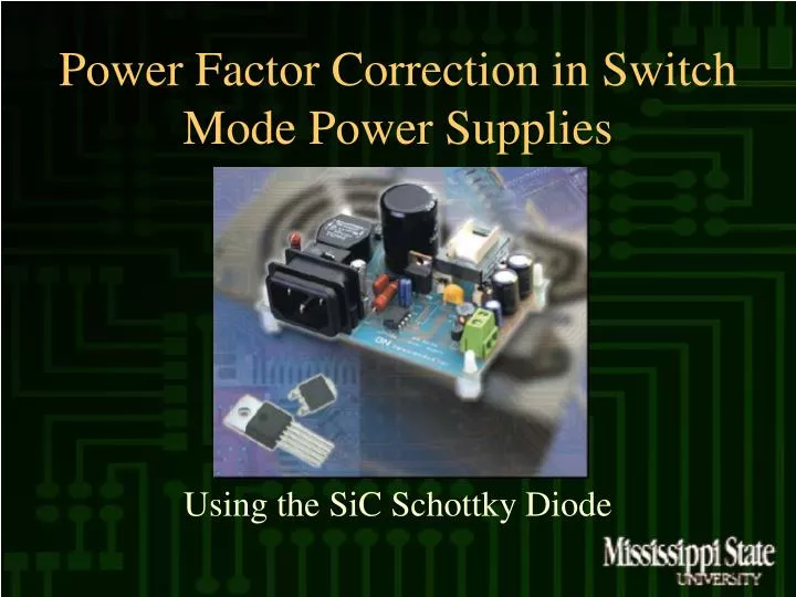
Power Factor Correction in Switch Mode Power Supplies Using the SiC Schottky Diode
Team • Team Leader • Robin Kelley • Team Members • Travis Brignac • Clinton Livingston • Advisor • Dr. Mazzola
Abstract • Design a switch mode power supply with a new power factor correction circuit, which implements the SiC Schottky diode. • Application of SMPS as an electronic ballast • Issue Application Note detailing use of the SiC Schottky diode in power factor correction
Comparison: Si pn vs. SiC Schottky • Reverse biased pn junction diode does not turn off fast enough during switching • This is due to the removal of excess carries from the depletion region • Causes reverse recovery transient • SiC Schottky diodes do not need to remove excess carries from the depletion region • Eliminates reverse recovery transient. • Allows for higher operating frequencies
System / Hardware 120V AC
Prototype Results Lamp Voltage f=200kHz Resistive Load f=100kHz
Current / Future Work • Debugging Stage of PFC • Second Design Phase of Inverter Circuit • Integrate major circuits • Final Testing
References • [1] H. Kapels, I. Zverev, R. Rupp, and L. Lorenz, “SiC Schottky diodes: A Milestone in hard switching applications,” Application Note, Infineon Technologies, 2001. • [2] Marco Scherf and Ilia Zverev, “200W SMPS Demonstration Board,” Application Note, Infineon Technology, v1.2, November 2001. • [3] M. Bairanzade, “Electronic Lamp Ballast Design,” Application Note, Motorola, 1995. • [4] “SWITCHMODEPower Supplies Reference Manual and Design Guide,” Manual, ON Semiconductor, Rev.3, July 2002. • [5] “Infineon Technologies Produces World’s first Power Semiconductors in Silicon Carbide,” http://www.infineon.com/news/press/102-019e.htm, Infineon Technologies AG, Muenchen,Germany, February 5, 2001 • [6] C. Miesner, R. Rupp, H. Kapels, M. Krach, and I. Zverev, “thinQ!™ Silicon Carbide Schottky Diodes: An SMPS Circuit Designer’s Dream Comes True!,” Technical White Paper, Infineon Technology, Infineon Technologies AG, September, 2001. • [7] Ming Hian Chew, “Design of Power Factor Correction Circuit Using GreenlineE Compact Power Factor Controller MC33260,” Application Note for AND8016/D, ON Semiconductor, June 2002. • [8] Product Information E2/32IS-120 Two Lamp Operation, 120V, Howard Industries, Inc., February 2001.