Download
1 / 10
160 likes | 522 Views
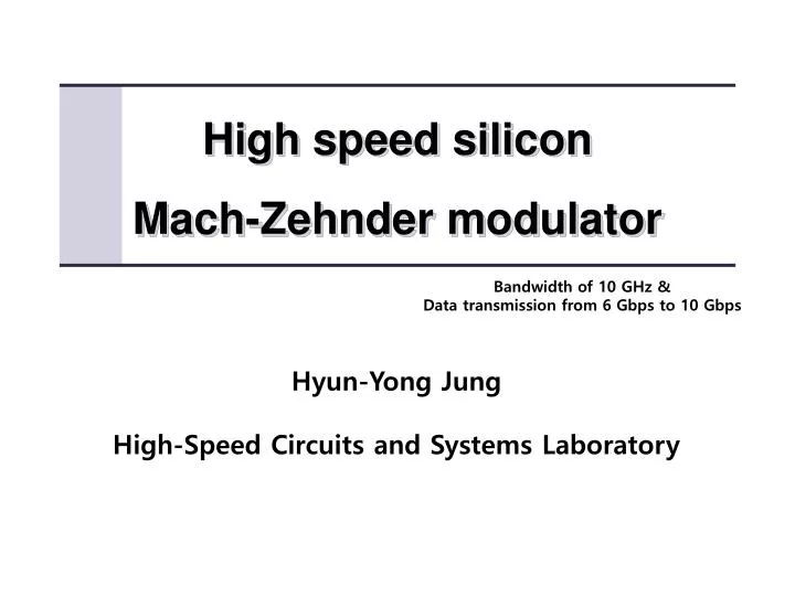
High speed silicon Mach- Zehnder modulator. Bandwidth of 10 GHz & D ata transmission from 6 Gbps to 10 Gbps. Hyun-Yong Jung High-Speed Circuits and Systems Laboratory. Outline. Introduction Device design Phase-shifter performance High speed data transmission Conclusion.

E N D
High speed silicon Mach-Zehnder modulator Bandwidth of 10 GHz & Data transmission from 6 Gbps to 10 Gbps Hyun-Yong Jung High-Speed Circuits and Systems Laboratory
Outline • Introduction • Device design • Phase-shifter performance • High speed data transmission • Conclusion
Introduction MOS Capacitor • Small signal BW : 2.5 GHz • Transmitting data : 1 GHz • - limited by driver • Transmitting data : 4 GHz • by customizing drive circuitry • Improvements in material quality, device design & driver circuitry • 10 Gbps data transmission, 3.8 dB ER & ~10 dB of on-chip loss
Device design 0.55 um p type-doped 1 um n type-doped • Epitaxial lateral overgrowth(ELO) is used to grow the crystalline Si • -ELO reduces the density of dislocations • Poly-Si ELO Si(crystalline-Si) • - Poly-Si is more lossy due to defects • To target high BW performance, the doping concentrations of Si are higher than those of previous poly-Si • To minimize the metal contact loss, design 2~3 um wide poly-Si pieces overlap the top corners of the ELO-Si rib
Device design • All wave guide dimensions are smaller than the first version • The optical mode is more tightly confined
Device design < Schematic of MZI, wire-bonds, and driver IC > • Overall length of the MZI modulator : 15 mm • -Each arm : 3.45 mm long high-doping • - High speed RF MOS capacitor phase shifter : 2~4.75 mm long lightly doped • - Low-speed phase shifters are driven with DC voltages to electrically • Driver Using 70 GHz-FT SiGe HBT process & employs a push-pull emitter-coupled logic output stage • Improved driver design & phase-shifter efficiency lead to reduced power dissipation
Phase-shifter performance N-type Si grounded P-type ELO-Si VD applied A thin charge layer on both side of the gate dielectric index(n) & absorption(α) of Si are changed neff changes • Optical phase shift depends on • neff changes, device length, and the optical wave length • Figure of merit (VπLπ) • – voltage swing & device length for π-radian phase shift • (0.15 π radian phase shift in this each MZI arm) • 7.8 V-cm 3.3 V-cm (minimizing shorten device length)
Phase-shifter performance • The intrinsic bandwidth (2πRC)-1 • (2πRC)-1 = 10.2 GHz
High speed data transmission • Optical eye diagram of modulator at λ = 1.55 um • Total insertion loss of 19 dB (10 dB - on chip, 9 dB - coupling) • Both eye diagrams have the same vertical and horizontal scales • Still slower than modulators based on LiNbO3 or III-V 40 GHz • This modulation can be more optimized • - Phase efficiency (MZI arm < 0.2 cm, on-chip loss < 2 dB) • - Higher BW can be obtained by increasing doping concentration W/ • higher loss
Conclusion • Efforts • Materials improvement • Optimization of dopant distribution • MZI splitter design to reduce on-chip loss • Incorporation of optical tapers to reduce coupling loss • Reduction of waveguide dimensions to scale phase modulation efficiency • Improvement of drive circuitry to realize higher data transmission • Results • Intrinsic bandwidth (as measured by RC cutoff) of 10 GHz • Driver-limited data transmission at 10 Gbps with 3.8 dB ER