Download
1 / 29
290 likes | 517 Views
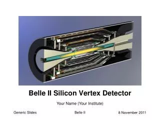
Silicon Vertex Detector at PHENIX. Physics Goal Detector Concept Structure Pixel detector Strip detector Summary. Atsushi Taketani RIKEN / RBRC. Physics with Silicon Vertex Tracker. QCD at high temperature Detail investigation of the hot and dense strongly interacting matter

E N D
Silicon Vertex Detector at PHENIX • Physics Goal • Detector Concept • Structure • Pixel detector • Strip detector • Summary Atsushi Taketani RIKEN / RBRC
Physics with Silicon Vertex Tracker QCD at high temperature • Detail investigation of the hot and dense strongly interacting matter • Energy loss of heavy quarks in the dense • Elliptic flow of heavy quarks • Open beauty production. • Accurate charm reference for quarkonium. • Determine QQ background of Thermal dilepton continuum • Improve Upsilon e+e- measurement Spin structure of nucleon • Gluon spin structure of the nucleon • Gluon polarization G/G with charm, beauty. • x dependence of G /G with -jet correlations. Key word = Heavy Quark production QCD in cold nuclei • Nuclear structure in nuclei • Nuclear dependence of PDFs. • Saturation physics: • Gluon shadowing over broad x-range
PhysicsGoals: Gluon polarization DG(x) Polarized p+p collisions Gluon polarization can be measured by doule-spin asymmetry A_LL of direct photon and heavy quark production in polarized pp collisions Jet + direct g constraint on xg Gluon Polarization • charm and bottom identification by displaced vertex • Jet identification with larger acceptance
Expected Performance D0 decay Collision Vertex Expected occupancy at Au-Au 200GeV most central event Distance to the Closest Approach [cm]
Gamma+jets dpT = 15 ⊕ 5.9pT % Q_h – jet_h
electrode h h h h h - P type + + - - + - + + - N type e e e e e electrode Sensor Diode What is Silicon Detector Charged particle electron Depletion Layer
Feature of Silicon Detector • High dE/dx ( ~ 2MeV /(g/cm^2) ) • Solid state detector comparing to gas chamber -> thin detector • Low e-h pair creation energy • 3.6 eV instead of 13.6 eV for gas chamber • Available Technology by industry • Compact, fine pitch and precise • Huge number of read out channel • Cost performance per readout channel
Details of sensor Strip Pixel Cross section • Huge readout channel • #ch ~ Surface area • True 2 dimensional read out • no ghost at all • Relatively small readout channel • #ch ~ (Surface area)^1/2 • 1+1 dimensional readout • ghost hits on high occupancy
Charmed meson ~ 100mm Bottomed meson~ 300mm Charmed or Bottomed messon Polarized Proton Polarized Proton Identifying long-lived particle Silicon detector
Requirements for Vertex Tracker Physics side • High precision tracking for displaced vertex measurement. 40mm displaced vertex resolution, ct ~ 100mm(D), ~400mm(B) • Large coverage tracking capability with momentum resolution (|h|<1.2 , and full azimuthally with s/P ~ 6%P) • High charged particle density ‘dN/dh’ ~ 700 @h=0 • High Radiation Dose ~3.3E12 Neutron/cm^2@10Years • High Luminosity @PP -> High rate readout • Low Material Budget <- avoid multiple scattering and photon conversion for electron measurement by outer detectors. Environment side
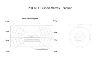
barrel VTX |h| < 1.2 NCC 0.9 < h < 3.0 Displaced vertex: VTX: silicon tracker FVTX: forward Si Jet measurement: NCC: nose cone calorimeter Other detectors: HBD: hadron blind detector Muon trigger PID in west arm Provides displaced vertex & jet measurement over 2p endcap VTX 1.2 < h < 2.7 HBD VTX NCC MuonTrig MuonTrig
The PHENIX VTX group • 92 people from 20 institutions as of 2006 May
Strip Pixel Structure • Barrel region • |h|<1.2, almost 2p in f • Pixel sensor at inner 2 layers • Strip sensors at outer 2 layers • Forward region • 1.2<|h|<2.7, 2p in f • 4 layers of mini strip • (50 x 2000 to 11000 mm) • Trigger capable R=10 and 14cm R=2.5 and 5cm
VTX parameters Pixel detector Strip detector BEAM Pixel Strip
Readout by ALICE_LHCB1 chip • Amp + Discriminator / channel • Bump bonded( 2 dim. Soldering) to each pixel • Running 10MHz clock ( RHIC 106nsec ) • Digital buffer for each channel > 4usec depth • Trigger capability > FAST OR logic for each crossing • 4 event buffer after L1 trigger PIXEL (Sensor and Readout) Pixel size( x z)50 µm x 425 µm Sensor Thickness 200um r = 1.28cm, z = 1.36 cm (Active area) 256 x 32 = 8192 channel / sensor 4 sensor/ chip 4 chip / stave
Half stave Full stave Pixel BUS Data 1.4cm 22cm Pixel detector module • Sensor module consists of 4 ALICE Pixel readout chips Bump-bonded to silicon sensor • One readout unit, half stave, made from two sensor modules • Half stave is mounted on the support structure • Pixel BUS to bring data out and send control signal into the readout chip is mounted on the half stave • Each detector module is built of two half staves,read out on the barrel ends Sensor Sensor Module Sensor Support structure + cooling ALICE LHCB1 chip
Pixel Readout Overview 45cm 11cm Half stave
Signal 1;(for Surface Mount Device) Signal-1, Signal-2, and signal-3 are connected with through hole Bus structure • 5 layers structure • GND, Power and 3 signal lines Wire bonding < 240 µm Final configuration sensor 200 µm (13 µm) Signal-1 3 mm Cu Readout chip 150 µm Signal-2 3 mm Cu Signal-3 3 mm Cu Signal 2;(Vertical line)line connected withpixel chip with wire bonding Power 50 mm Al Signal 3;(Horizontal line)send signal to Pilot Module connected with vertical line with through hole GND 50 mm Al Line spacing; 70 mm pitch Material Budget; Total ~ 0.26 %
Readout pictures Extender Pixel Ladder SPIRO FEM
Set-up of three layers 2. Set-up of the telescope • Three half staves • Three SPIROs • One FEM • Two trigger scintillator • Analysis software • DAQ • Data converter • Tracking code • Event display
Event# 200 Layer 1 chip 4 chip 3 chip 2 chip 1 Layer 2 chip 8 chip 7 chip 6 chip 5 Layer 3 chip 12 chip 11 chip 10 chip 9 row column
Silicon Sensor Stripixel Concept • a-pixels are connected to form X-strips, and b-pixels are connected to form stereo-angled (4.6o) U-strips b-pixels interconnect X strips (connect a-pixels) a-pixels interconnect u strips (connect b-pixels) Readout pulse height by ADC
Sensor elements: Two strip-pixel arrays on a single-sided wafer of 500 µm thickness, with 384 + 384 channels on 3 x 3 cm2 area. Initial design: “longitudinal” readout. Made by SINTEF Pixels: 80 µm 1 mm, projective readout via double metal XU/V “strips” of ~3 cm length. new design: “lateral” SVX4 readout. Made by Hamamatsu Developed at BNL Instrumentation Gr. • Single sided • 1+1 dimensional readout ( X and U direction) • 3cmx3cm sensor x2 / chip • 768 X strip and 768 U strips/chip Position resolution is 25mm by test beam
The 1st prototype detector 625 μm thickness Tested at BNL ROC+RCM+FEM prototype w/ SVX4 chips developed by ORNL Gluing/wire-bonding at RIKEN Prototype Detector Using HPK Sensor XYZ micro-stage Power cables Optical fiber + focuser Bias line Data + Control cables
S/N ~ 20:1 for 625 μm thickness Charge-sharing test w/ IR laser pulse injection Large spot size in the present setup Focusing length (8 mm) was too short to shine only one pixel in 625 μm thick sensor. The maximum focusing length available in the same company is 70 mm. Not enough. Planned: possible solution is to use a radioactive source, cosmic rays and beam. X3R U3R IR Laser Tests Results Laser spot X-Strip U-Strip U-Strip
R&D : Prototypes Sensors • 1st prototype sensor • Spiral p+ electrode : 8 μm line, 5 μm gap, 3 turns • Thickness : 400/250 μm • R/O chip: VA2 (analog multiplexer) • Tests w/ source & beam • S/N: 17:1 for 400 μm thickness • 2-D sensitivity need improvements. 1st prototype sensor • 2nd prototype sensor • Spiral p+ electrode : 5 μm line, 3 μm gap, 5 turns • Thickness : 400/500 μm • R/O chip: SVX4(CDF SVX4 hybrid) • Tests w/ nano-sec pulsed laser • S/N: 14:1 for 500 μm thickness • Laser signals were seen 2nd prototype sensor
Saturation of circuit 15nA/strip Radiation damage of stripixel sensor PHENIX in RHIC2 for 10 years 3.3E+12 [Neq/cm2] for 1 year from 2009 ~3E+11 [Neq/cm2] Rikkyo 20 ℃ 10 ℃ 0 ℃ -10 ℃ PHENIX IR Operation temperature will be 0 deg C
Summary • PHENIX VTX will investigate many physics on both spin and heavy ion program of RHIC. • Detector R&D and production is on going. • VTX will be installed in 2009. • You are welcome to visit our Lab@RIKEN.
barrel VTX |h| < 1.2 NCC 0.9 < h < 3.0 Displaced vertex: VTX: silicon tracker FVTX: forward Si Jet measurement: NCC: nose cone calorimeter Other detectors: HBD: hadron blind detector Muon trigger PID in west arm Provides displaced vertex & jet measurement over 2p endcap VTX 1.2 < h < 2.7 HBD VTX NCC MuonTrig MuonTrig