Download
1 / 34
340 likes | 414 Views
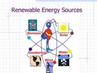
Power Generation from Renewable Energy Sources. Fall 2012 Instructor: Xiaodong Chu Email : chuxd@sdu.edu.cn Office Tel.: 81696127. Flashbacks of Last Lecture.

E N D
Power Generation from Renewable Energy Sources Fall 2012 Instructor: Xiaodong Chu Email:chuxd@sdu.edu.cn Office Tel.: 81696127
Flashbacks of Last Lecture • We could compute monthly and annual clear sky insolation on collectors with various azimuth and tilt angles, as well as for one- and two-axis tracking mounts for different latitudes
Flashbacks of Last Lecture • Creation of solar energy databases is achieved by using measurement sites while incorporating meteorological data such as cloud mapping taken by satellite, as an important complement to the sparse global network of ground monitoring stations • There are two principal types of devices used to measure solar radiation: pyranometer and pyrheliometer
Flashbacks of Last Lecture • How to estimate the average insolation that can be expected to strike a collector under real conditions at a particular site? • Site-specific, long-term radiation data are required, which is primarily insolation measured on a horizontal surface • Sort out what portion of the total measured horizontal insolation is diffuse and what portion is direct beam • Convert horizontal beam radiation • Adjust the resulting horizontal diffuse radiation into diffuse and reflected radiation on a collecting surface
Photovoltaic Materials and Electrical Characteristics–Introduction • A material or device that is capable of converting the energy contained in photons of light into an electrical voltage and current is said to be photovoltaic • A photon with short enough wavelength and high enough energy can cause an electron in a photovoltaic material to break free of the atom that holds it • If a nearby electric field is provided, those electrons can be swept toward a metallic contact where they can emerge as an electric current • The driving force to power photovoltaics comes from the sun
Photovoltaic Materials and Electrical Characteristics–Introduction • The history of photovoltaics (PVs) began in 1839 when a French physicist, Edmund Becquerel, caused a voltage to appear when he illuminated a metal electrode in a weak electrolyte solution • Almost 40 years later, Adams and Day were the first to study the photovoltaic effect in solids • Albert Einstein published a theoretical explanation of the photovoltaic effect in 1904, which led to a Nobel Prize in 1923 • About the same time, a Polish scientist Czochralski began to develop a method to grow perfect crystals of silicon • By the 1940s and 1950s, the Czochralski process began to be used to make the first generation of single-crystal silicon photovoltaics, and that technique continues to dominate the PV industry today
Photovoltaic Materials and Electrical Characteristics–Introduction • In the 1950s there were several attempts to commercialize PVs, but their cost was prohibitive • The real emergence of PVs as a practical energy source came in 1958 when they were first used in space for the Vanguard I satellite • For space vehicles, cost is much less important than weight and reliability, and solar cells have ever since played an important role in providing onboard power for satellites and other space craft • Spurred on by the emerging energy crises of the 1970s, the development work supported by the space program began to pay off back on the ground
Photovoltaic Materials and Electrical Characteristics–Introduction Best laboratory PV cell efficiencies for various technologies
Photovoltaic Materials and Electrical Characteristics–Basic Semiconductor Physics • Photovoltaics use semiconductor materials to convert sunlight into electricity • The technology for doing so is very closely related to the solid-state technologies used to make transistors, diodes, and all of the other semiconductor devices • The starting point for most of the world’s current generation of photovoltaic devices is pure crystalline silicon, which is in the fourth column of the periodic table, which is referred to as Group IV • Boron and phosphorus are added to silicon to make most PVs • Gallium and arsenic are used in GaAs solar cells, while cadmium and tellurium are used in CdTe cells
Photovoltaic Materials and Electrical Characteristics–Basic Semiconductor Physics
Photovoltaic Materials and Electrical Characteristics–Basic Semiconductor Physics • Silicon has 14 protons in its nucleus, and so it has 14 orbital electrons • Its outer orbit contains four valence electrons—that is, it is tetravalent • Those valence electrons are the only ones that matter in electronics, so it is common to draw silicon as if it has a +4 charge on its nucleus and four tightly held valence electrons, as shown
Photovoltaic Materials and Electrical Characteristics–Basic Semiconductor Physics • At absolute zero temperature, silicon is a perfect electrical insulator • As the temperature increases, some electrons will be given enough energy to free themselves from their nuclei, making them available to flow as electric current • The warmer it gets, the more electrons there are to carry current, so its conductivity increases with temperature • Silicon’s conductivity at normal temperatures is still very low, and so it is referred to as a semiconductor • By adding minute quantities of other materials, the conductivity of pure semiconductors can be greatly increased
Photovoltaic Materials and Electrical Characteristics–Basic Semiconductor Physics • Energy bands for semiconductors • Electrons have energies that must fit within certain allowable energy bands • The top energy band is called the conduction band, and it is electrons within this region that contribute to current flow • The conduction band for metals is partially filled, but for semiconductors at absolute zero temperature, the conduction band is empty • At room temperature, only about one out of 1010 electrons in silicon exists in the conduction band
Photovoltaic Materials and Electrical Characteristics–Basic Semiconductor Physics • The gaps between allowable energy bands are called forbidden bands, the most important of which is the gap separating the conduction band from the highest filled band below it • The energy that an electron must acquire to jump across the forbidden band to the conduction band is called the band-gap energy, Eg
Photovoltaic Materials and Electrical Characteristics–Basic Semiconductor Physics • The band-gap Eg for silicon is 1.12 eV, which means an electron needs to acquire that much energy to free itself from the electrostatic force that ties it to its own nucleus—that is, to jump into the conduction band • Where might that energy come from? • For photovoltaics, the energy source is photons of electromagnetic energy from the sun • When a photon with more than 1.12 eV of energy is absorbed by a solar cell, a single electron may jump to the conduction band
Photovoltaic Materials and Electrical Characteristics–Basic Semiconductor Physics • When a single electron may jump to the conduction band, it leaves behind a nucleus with a +4 charge that now has only three electrons attached to it • There is a net positive charge, called a hole, associated with that nucleus • Unless there is some way to sweep the electrons away from the holes, they will eventually recombine, obliterating both the hole and electron
Photovoltaic Materials and Electrical Characteristics–Basic Semiconductor Physics • A valence electron in a filled energy band can easily move to fill a hole in a nearby atom, without having to change energy bands • The hole, in essence, moves to the nucleus from which the electron originated • Electric current in a semiconductor can be carried not only by negatively charged electrons moving around, but also by positively charged holes that move around as well
Photovoltaic Materials and Electrical Characteristics–Basic Semiconductor Physics • Photons with enough energy create hole–electron pairs in a semiconductor • Photons can be characterized by their wavelengths or their frequency as where c is the speed of light (3 × 10⁸ m/s), v is the frequency (hertz), λ is the wavelength (m), and where E is the energy of a photon (J) and h is Planck’s constant (6.626 × 10⁻³⁴ J-s)
Photovoltaic Materials and Electrical Characteristics–Basic Semiconductor Physics • For a silicon photovoltaic cell, photons with wavelength greater than 1.11 μm have energy less than the 1.12-eV band-gap energy needed to excite an electron • None of those photons create hole–electron pairs capable of carrying current, so all of their energy is wasted • Photons with wavelengths shorter than 1.11 μm have more than enough energy to excite an electron • Since one photon can excite only one electron, any extra energy above the 1.12 eV needed is dissipated as waste heat in the cell
Photovoltaic Materials and Electrical Characteristics–Basic Semiconductor Physics
Photovoltaic Materials and Electrical Characteristics–Basic Semiconductor Physics • Assuming a standard air mass ratio AM 1.5, 20.2% of the energy in the spectrum is lost due to photons having less energy than the band gap of silicon (hν < Eg), and another 30.2% is lost due to photons with hν > Eg • The remaining 49.6% represents the maximum possible fraction of the sun’s energy that could be collected with a silicon solar cell under 50%
Photovoltaic Materials and Electrical Characteristics–Basic Semiconductor Physics • With a smaller band gap, more solar photons have the energy needed to excite electrons, which is good since it creates the charges that will enable current to flow • A small band gap means that more photons have surplus energy above the threshold needed to create hole–electron pairs, which wastes their potential • A high band gap means that fewer photons have enough energy to create the current carrying electrons and holes, which limits the current that can be generated • A high band gap gives those charges a higher voltage with less leftover surplus energy
Photovoltaic Materials and Electrical Characteristics–Basic Semiconductor Physics • Low band gap gives more current with less voltage while high band gap results in less current and higher voltage • Since power is the product of current and voltage, there must be some middle-ground band gap, usually estimated to be between 1.2 eV and 1.8 eV, which will result in the highest power and efficiency
Photovoltaic Materials and Electrical Characteristics–Basic Semiconductor Physics • Besides two fundamental constraints, other factors that contribute to the drop in theoretical efficiency include • Only about half to two-thirds of the full band-gap voltage across the terminals of the solar cell • Recombination of holes and electrons before they can contribute to current flow • Photons that are not absorbed in the cell either because they are reflected off the face of the cell, or because they pass right through the cell, or because they are blocked by the metal conductors that collect current from the top of the cell • Internal resistance within the cell, which dissipates power
Photovoltaic Materials and Electrical Characteristics–Basic Semiconductor Physics • To avoid recombination, electrons in the conduction band must continuously be swept away from holes • In PVs this is accomplished by creating a built-in electric field within the semiconductor itself that pushes electrons in one direction and holes in the other • To create the electric field, two regions are established within the crystal • On one side of the dividing line separating the regions, pure silicon is purposely contaminated with very small amounts of a trivalent element from column III of the periodic chart; on the other side, pentavalent atoms from column V are added
Photovoltaic Materials and Electrical Characteristics–Basic Semiconductor Physics • Consider the side of the semiconductor that has been doped with a pentavalent element such as phosphorus • An atom of the pentavalent impurity forms covalent bonds with four adjacent silicon atoms • Only about 1 phosphorus atom per 1000 silicon atoms is typical • Four of its five electrons are now tightly bound, but the fifth electron is left on its own to roam around the crystal • When that electron leaves the vicinity of its donor atom, there will remain a +5 donor ion fixed in the matrix surrounded by only four negative valence electrons • Each donor atom can be represented as a single, fixed, immobile positive charge plus a freely roaming negative charge
Photovoltaic Materials and Electrical Characteristics–Basic Semiconductor Physics • Since there are now negative charges that can move around the crystal, a semiconductor doped with donor atoms is referred to as an n-type material
Photovoltaic Materials and Electrical Characteristics–Basic Semiconductor Physics • On the other side of the semiconductor, silicon is doped with a trivalent element such as boron • The concentration of dopants is small, something on the order of 1 boron atom per 10 million silicon atoms • These dopant atoms fall into place in the crystal, forming covalent bonds with the adjacent silicon atoms • Since each of these impurity atoms has only three electrons, only three of the covalent bonds are filled, which means that a positively charged hole appears next to its nucleus • An electron from a neighboring silicon atom can easily move into the hole, so these impurities are referred to as acceptors since they accept electrons • The filled hole now means there are four negative surrounding a +3 nucleus • All four covalent bonds are now filled creating a fixed, immobile net negative charge at each acceptor atom
Photovoltaic Materials and Electrical Characteristics–Basic Semiconductor Physics • Each acceptor has created a positively charged hole that is free to move around in the crystal, so this side of the semiconductor is called a p-type material
Photovoltaic Materials and Electrical Characteristics–Basic Semiconductor Physics • Suppose we put an n-type material next to a p-type material forming a junction between them • In the n-type material, mobile electrons drift by diffusion across the junction • In the p-type material, mobile holes drift by diffusion across the junction in the opposite direction • When an electron crosses the junction it fills a hole, leaving an immobile, positive charge behind in the n-region, while it creates an immobile, negative charge in the p-region • These immobile charged atoms in the p and n regions create an electric field that works against the continued movement of electrons and holes across the junction • As the diffusion process continues, the electric field countering that movement increases until eventually (actually, almost instantaneously) all further movement of charged carriers across the junction stops
Photovoltaic Materials and Electrical Characteristics–Basic Semiconductor Physics • The exposed immobile charges creating the electric field in the vicinity of the junction form what is called a depletion region, meaning that the mobile charges are depleted—gone—from this region • The width of the depletion region is only about 1 μm and the voltage across it is perhaps 1 V, which means the field strength is about 10,000 V/cm
Photovoltaic Materials and Electrical Characteristics–Basic Semiconductor Physics • The voltage–current characteristic curve for the p–n junction diode is described by the following Shockley diode equation where Id is the diode current in the direction of the arrow (A), Vd is the voltage across the diode terminals from the p-side to the n-side (V), I0 is the reverse saturation current (A), q is the electron charge (1.602 × 10⁻¹⁹C), k is Boltzmann’s constant (1.381 × 10⁻²³ J/K), and T is the junction temperature (K)
Photovoltaic Materials and Electrical Characteristics–Basic Semiconductor Physics • Substituting the above constants into the exponent of (8.3) gives • A junction temperature of 25◦C is often used as a standard, which results in the following diode equation
Photovoltaic Materials and Electrical Characteristics–Basic Semiconductor Physics • Examples 8.1 and 8.2 of the textbook: you should master them!