Download
1 / 28
280 likes | 361 Views
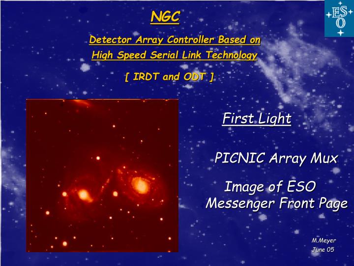
NGC. Detector Array Controller Based on. High Speed Serial Link Technology. First Light PICNIC Array Mux Image of ESO Messenger Front Page. [ IRDT and ODT ]. M.Meyer June 05. Conventional Approach : Acquisition System (IRACE). PCI Interface. Communication and Data Transfer.

E N D
NGC Detector Array Controller Based on High Speed Serial Link Technology First Light PICNIC Array Mux Image of ESO Messenger Front Page [ IRDT and ODT ] M.Meyer June 05
Conventional Approach :Acquisition System (IRACE) PCI Interface Communication and Data Transfer Acquisition Module(s) Sequencer Clock and Bias
NGC Prototype - Minimum SystemBack-End and Front-End ( Four Channels ) • NGC is a modular system for IR detector and CCD readout with a Back-end, a basic Front-end unit containing a complete four channel system on one card and additional boards like multi channel ADC units and more... • There is no processor, no parallel inter-module data bus on the front-end side. Advanced FPGA link technology is used to replace conventional logic • Connection between Back and Front-end with high speed fiber links at 2.5GBit/s • Connection between Front-end modules with high speed copper links at 2.5GBit/s. • Power Consumption on this Front-end is less than 10 Watts ( Excluding power supply ) • This Front-End system does not require big cooling boxes
System Noise on Prototype 2 1 4 3
Back-End VirtexII Pro Contains : PCI 64 IF (IP) Communication DMA Data Transfer Fiber optics
Back-End • Function is based on the XILINX Virtex Pro FPGA XC2VP7 FF 672 • Back-End PCI is a 64 Bit PCI board • FPGA contains PCI interface to Communication functions DMA data channel Status and Command • Direct interface from FPGA to PCI without glue logic • PCI master and PCI slave are independent • Scatter – Gather DMA implemented • Communication and data transfers all on serial link with RocketIO transceivers • Handshake communication to Front-End • Data rate on one channel between front and back-end ~ 200MByte/s
Acquisition 4 Channels 16/18 Bit Monitoring Telemetry 16 Bit Front-End VirtexII Pro Contains : Communication Data transfer Sequencer Telemetry Glue logic CLOCK and BIAS
Front-End • Function is based on the XILINX Virtex Pro FPGA XC2VP7 FF 672 • FPGA contains link interface for communication and data transfer with RocketIO transceivers, sequencer, system administration, interface to acquisition, clock and bias, telemetry and monitoring • Four ADC channels ( 16 or 18Bit) • 16 clocks, 20 biases • Telemetry • Monitoring • Data rate on one channel between front-end modules and front to back-end ~ 200MByte • Handshake for communication to back-end • Galvanic isolated trigger input and control outputs • Connection to detector ASIC’s - all communication and data transfer to the back-end can be handled with the same firmware already contained in the FPGA
Virtex Pro Internals Device utilization summary: Selected Device : 2vp7ff672-5 Number of Slices: 2508 out of 4928 50% Number of Slice Flip Flops: 3043 out of 9856 30% Number of 4 input LUTs: 4190 out of 9856 42% Number of bonded IOBs: 124 out of 396 31% Number of TBUFs: 160 out of 2720 5% Number of BRAMs: 25 out of 44 56% Number of GCLKs: 3 out of 16 18% Number of GTs: 4 out of 8 50% Number of DCMs: 1 out of 4 25% Signals to route : 22530 Used language : VHDL
Communication and Data Transfer • Communication and data transfer is handled with the Virtex Pro FPGA’s Gigabit transceivers • The communication between all system modules is based on packet transmission over serial links • A packet structure is defined to address a function ( e.g. a register or memory in a front-end module) for read or write • From the Back-End ( PCI board ) the packets can be routed to and through each board in the Front-End • Data are routed with the same structure from the acquisition modules to the Back-End
Basic System Basic System
NGC Detector Array Controller Based on High Speed Serial Link Technology Two Posters on the same Topic NGC Front-end for CCDs and AO applications - Javier Reyes Software for the New Generation Detector Controller - Claudio Cumani M.Meyer June 05
Engineers Bad Days or The Real World
How many Errors will be on ?It’s a 10 Layer board with BGA’s !
Front-End Basic BoardSequencer Module • Sequencer is completely contained within the FPGA • 100MHz design = 10ns resolution • Firmware interpreter for Sequencer Codes within the FPGA • Galvanic isolated high speed trigger input and control outputs Sequencer Codes 000 Stop Interpreter Stops Pattern Interpretation 001 EXEC Pattern < Number of Pattern, Number of Repetitions > 010 LOOP < Number of Repetitions > 011 LOOP END 100 LOOP INFINITE 101 JUMP SUBROUTINE < Address > 110 RETURN SUBROUTINE 111 Reserved