Download
1 / 46
530 likes | 1.44k Views
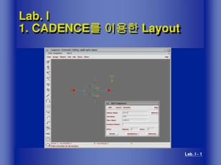
Chapter 3 Cadence ® Analog Design Environment. Getting started with Cadence Tool Schematic Editor Layout Tutorial Introduction to Verilog-A Cadence tool information @ http://www.cadence.com/datasheets/. Getting Started with Cadence Tool.

E N D
Chapter 3 Cadence® Analog Design Environment Getting started with Cadence Tool Schematic Editor Layout Tutorial Introduction to Verilog-A Cadence tool information @ http://www.cadence.com/datasheets/ Chap 3, Cadence Analog Artist Design Environment, ELEC6970, FDAI, 2004
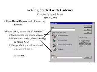
Getting Started with Cadence Tool • Install cadence tool: under UNIX, user services user setup Electronics Data Analysis (EDA) eda/cadence/1.0 • Setup cadence tool: under UNIX, mkdir Name6970, download .cdsenv, .cdsinit, and cds.lib from WebCT/References to Name6970. • Add the following in your .cshrc file: setenv CDS_Netlisting_Mode "Analog " • Launch Cadence: in “Name6970” by typing icfb& or icms& or msfb • Cadence Manu: pdf files @/opt/cadence/ic4.46/doc, use help or type “openbook&” under UNIX. Chap 3, Cadence Analog Artist Design Environment, ELEC6970, FDAI, 2004
Design System Initialization Files • .cshrc and .login configure the operating system environment and the UNIX environment when you login and start a UNIX application. • .cdsinit customizes the Affirma Analog Circuit Design Environment. • .cdsenv configure Cadence Analog Artist tool environment. • cds.lib set paths to the libraries used by the Analog Artist software. Cadence default lib: INCLUDE /opt/cadence/ic4.46/share/cdssetup/cds.lib User defined lib: DEFINE Dai6970 /export/daifa01/cadence/Dai6970 • Cadence process design kit (PDK) can be downloaded @www.cadencePDK.com Chap 3, Cadence Analog Artist Design Environment, ELEC6970, FDAI, 2004
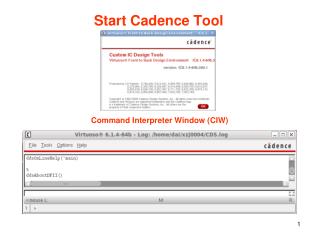
Start Cadence Tool • icfb& front to back design, default CDS_Netlisting_Mode “Digital“ • icms& mixed signal design, default CDS_Netlisting_Mode “Digital“ • msfb& mixed signal front to back design, default CDS_Netlisting_Mode “Analog“, don’t need to add setenv CDS_Netlisting_Mode "Analog “ in .cshrc. • Schematic cellview to cellview defaults for creating a symbol with Artist. The default is to not create an Artist symbol. The following has been added in .cdsinit: schSetEnv( "tsgTemplateType" "artist" ) Chap 3, Cadence Analog Artist Design Environment, ELEC6970, FDAI, 2004
Start Cadence Tool Command Interpreter Window (CIW) Chap 3, Cadence Analog Artist Design Environment, ELEC6970, FDAI, 2004
Initializing Design Framework II Environment The Design Framework II software reads your .cdsinit file at startup to set up your environment. .cdsinit: Sets user-defined bindkeys. Redefines system-wide defaults. Contains SKILL commands. The search order for the .cdsinit file is: <Filename><install_dir>/tools/dfII/local the current directory [Name6970] put .cdsenv, .cdsinit, cds.lib here the home directory When a .cdsinit file is found, the search stops unless a command in .cdsinit reads other files. Path to a sample .cdsinit file: <Filename><install_dir>/tools/dfII/samples/artist/cdsinit <install_dir>=/opt/cadence/ic4.46 Chap 3, Cadence Analog Artist Design Environment, ELEC6970, FDAI, 2004
Library Manager CIW: Tools -> Library Manager. Chap 3, Cadence Analog Artist Design Environment, ELEC6970, FDAI, 2004
Library Manager -- View • schematic- contains the logical design of the device. • symbol- contains the symbol representation of the schematic. • layout - contains the silicon -level representations of the transistors and wiring. • CdsSpice, HspiceS, Spectre, spectreS–contain spice information for the element. • abstract- contains an abstract representation of the layout for use by Cadence place and route software. • extracted - contains layout connectivity for use by verification programs. • behavioral –contains the VHDL description of the cell Chap 3, Cadence Analog Artist Design Environment, ELEC6970, FDAI, 2004
Features in Cadence Design Environment Virtuoso Composer for schematic capture, Analog Environment for simulation, Virtuoso Layout for layout, Diva for DRC (design rule checking), Diva for extraction, Diva for LVS (layout vs. schematic), Analog Environment for postlayout simulation Chap 3, Cadence Analog Artist Design Environment, ELEC6970, FDAI, 2004
Schematic Entry Flow Open Design Add Component Instances Add Pins Add and Name Wires Check Save Symbol Editor Chap 3, Cadence Analog Artist Design Environment, ELEC6970, FDAI, 2004
Schematic Editor Bindkey Chart Chap 3, Cadence Analog Artist Design Environment, ELEC6970, FDAI, 2004
Symbol Editor Bindkey Chart Chap 3, Cadence Analog Artist Design Environment, ELEC6970, FDAI, 2004
General Bindkey Chart Chap 3, Cadence Analog Artist Design Environment, ELEC6970, FDAI, 2004
Mouse Buttons Bindkey Chart Chap 3, Cadence Analog Artist Design Environment, ELEC6970, FDAI, 2004
Chapter 3 Cadence® Analog Design Environment Layout Tutorial Chap 3, Cadence Analog Artist Design Environment, ELEC6970, FDAI, 2004
SETUP 1. Attach your design library to technology library In the CIW window >>Technology file>>Attach to>> 2 .You have to load the display resource file in the directory cadence is installed In the CIW >>Tools>>Display Resources>>Merge files …select technology/display.drf Your Destination DRF should be the path where cadence is stored/display.drf Display resource file contains the display settings for your layout (i.e colours for different layers and via’s etc). Chap 3, Cadence Analog Artist Design Environment, ELEC6970, FDAI, 2004
Next select a schematic you wish to layout. From the library manager >>file>>create new file>>… Cell name::diffamp View name::layout Tool:: Virtuoso Chap 3, Cadence Analog Artist Design Environment, ELEC6970, FDAI, 2004
Having done that , two new windows open. Note ## If all the layers in LSW are black in colour , it means that your Display.drf has not been loaded properly. Note## Also make sure that the library name appearing on the LSW window is technology. If everything is fine your screen should look like this… Layer selection window Current layer Current library AV = all layers visible NV = none visible AS = All select NS = none select dg = drawing (type you use the most) pn = pin (used for creating pins) br used for large via’s. Layers Note## only way to close this window is to exit from cadence Chap 3, Cadence Analog Artist Design Environment, ELEC6970, FDAI, 2004
Layout editing window ruler path properties rectangle instance path polygon polygon label rectangle ruler Chap 3, Cadence Analog Artist Design Environment, ELEC6970, FDAI, 2004
Metal Options metal4 MT metal3 AM metal1 metal2 Chap 3, Cadence Analog Artist Design Environment, ELEC6970, FDAI, 2004
Via’s and Metallization options via1 via4 via1 Via are used for transferring from one metal layer to another via2 via2 AV via3 via3 5 Level Metal MC CAM1V1M2V2M3 V3MT AVAM 4 Level Metal MC -->CA --> M1 --> V1 --> M2 --> V2 --> MT --> AV --> AM -->===(Q) **Use of Q provides an optional metal-insulator-metal capacitor Chap 3, Cadence Analog Artist Design Environment, ELEC6970, FDAI, 2004
Reshape objects Merge Objects Merge objects ofsame layer only Chap 3, Cadence Analog Artist Design Environment, ELEC6970, FDAI, 2004
More on LSW:: Layer names:: ca metal one to polysilicon contact mc metal contact rx thin oxide layer nw n-well (used for p-fets) dt deep trench used to isolate n-well around pfet pc polysilicon , used for gates and interconnecting gates m1 metal 1 lowest metal layer v1 via connects m1 to m2 m2,m3,m4 other metal layers v2,v3,v4 other interconnect via’s Chap 3, Cadence Analog Artist Design Environment, ELEC6970, FDAI, 2004
Grid size and display options Gridcontrols Display levels Chap 3, Cadence Analog Artist Design Environment, ELEC6970, FDAI, 2004
Then select tools>>layout xl..the schematic window opens . Then select design>>gen from source …the tool automatically places the layout views of individual devices, with out their interconnections., this is useful for large designs. Chap 3, Cadence Analog Artist Design Environment, ELEC6970, FDAI, 2004
Chap 3, Cadence Analog Artist Design Environment, ELEC6970, FDAI, 2004
How ever in this case for a differential pair , we can place the transistors ourselves , since the design is not complicated. Press i for create instance , then select your transistor technology library and place them on the layout editing window. Note## change the display levels from 0 to 32…see previous slides Magnification=25 !!! similarly place other components that are in your schematic. Having done so the next step is to wire your devices Chap 3, Cadence Analog Artist Design Environment, ELEC6970, FDAI, 2004
PNP NPN base emitter collector base emitter collector Chap 3, Cadence Analog Artist Design Environment, ELEC6970, FDAI, 2004
The blue lines show the metal 1 connections between the devices. To draw a metal connection , select m1 dg in the Layer selection window. Then in the layer editing window select path and click on two points to draw a path between two points. Here I have selected metal 2 for my pins. So first put an via v1 between metal 1 and metal 2 , for this select v1 dg in the layer selection window. In the layout editing window select rectangle and draw an rectangular via on metal 1. Next on top of this we have to put an metal 2 pin. For this select m2 pn in the LSW and draw the pin as shown below on the v1 via. Next press ctrl+p to create a symbolic pin , a window opens up as shown below , type in the pin name , select pin type as M2_T in this case, click on display pin name button and move the yellow square you see on top of the m2 pn pink rectangle. metal1 metal2 via1 Metal2 pin Chap 3, Cadence Analog Artist Design Environment, ELEC6970, FDAI, 2004
Pins • Choose create >>pin>>..and a window will open • If the window is titled “create pin shape”, choose “sym pin” under mode option • Enter a terminal name • Specify the “I/O type” • Specify the pin type as metal1 or metal2,..depending on which is the top layer at the place that the pin is to be inserted (they should match) • Specify the pin width Chap 3, Cadence Analog Artist Design Environment, ELEC6970, FDAI, 2004
PINS Chap 3, Cadence Analog Artist Design Environment, ELEC6970, FDAI, 2004
Pins Note## Pin names in layout and schematic must match exactly (case sensitive) Chap 3, Cadence Analog Artist Design Environment, ELEC6970, FDAI, 2004
Design Rule Checking To perform design rule checking select verify>>DRC ..and a DRC window opens up, select OK to begin DRC DRC Window Chap 3, Cadence Analog Artist Design Environment, ELEC6970, FDAI, 2004
The results of the DRC are displayed in the CIW window. If you have no errors then your window should look like the one above. The minimum number of errors you get is 2 , they are actually not any errors. If you have violated any design rules then the rules violated are shown as below. i.e here rules no. 550 , 570 , 575 have been violated. Chap 3, Cadence Analog Artist Design Environment, ELEC6970, FDAI, 2004
Layout Verification For performing LVS you have to extract the layout first . This is done as follows:: Select verify >>extract>> …extract window opens up , type in the rules file as divaEXT4.rul , and select OK , as shown below. Extractorwindow Chap 3, Cadence Analog Artist Design Environment, ELEC6970, FDAI, 2004
Once extraction is complete check you CIW , it should look like this:: Also a new cell view of type extracted is created in your library. Chap 3, Cadence Analog Artist Design Environment, ELEC6970, FDAI, 2004
Your cell view extracted looks like this , the green back ground is the substrate Chap 3, Cadence Analog Artist Design Environment, ELEC6970, FDAI, 2004
To run LVS select verify>>LVS>> LVS for window opens, the views in LVS form should be schematic and extracted. If you get a window saying LVS forms content open then just click OK Click RUN to start LVS. schematic extracted divaLVS.rul technology click on the output on LVS window to see the results of LVS run It should have the line “the net lists match” if everything is you should hopefully get a window saying this:: Chap 3, Cadence Analog Artist Design Environment, ELEC6970, FDAI, 2004
click on the output on LVS window to see the results of LVS run It should have the line “the net lists match” if everything is fine Chap 3, Cadence Analog Artist Design Environment, ELEC6970, FDAI, 2004
COMPONENTS OF DIVA VERIFICATION • Diva Design Rule Checker (DRC) • Diva Layout vs. Schematic (LVS) Verifier (includes electrical rule checks (ERC) and extraction of device layout parameters) • Diva Parasitic Extractor (RCX) • Diva Physical Verification Suite (consists of Diva DRC and Diva LVS) • Diva Physical Verification and Extractor Suite (consists of Diva DRC, Diva LVS, and Diva RCX) Chap 3, Cadence Analog Artist Design Environment, ELEC6970, FDAI, 2004
Introduction to Verilog-A Verilog-A -- Combinational: XOR Gate `include "discipline.h" // discipline.h contains definitions for the standard natures and // disciplines such as electrical disciplines.`include "constants.h" // constants.h contains commonly used mathematical and physical // constants such as PI and Boltzman’s constants.// - xor gate//// vin1, vin2: [V,A]// vout: [V,A]//// INSTANCE parameters// vlogic_high = output voltage for high [V]// vlogic_low = output voltage for high [V]// vtrans = voltages above this at input are considered high [V]// tdel, trise, tfall = {usual} [s] Chap 3, Cadence Analog Artist Design Environment, ELEC6970, FDAI, 2004
Verilog-A -- Combinational: XOR Gate module xor_gate(vin1, vin2, vout);input vin1, vin2;output vout;electrical vin1, vin2, vout; //potential and flow are associated with // voltageand current for type electrical.parameter real vlogic_high = 3.3;parameter real vlogic_low = 0;parameter real vtrans = 1.5;parameter real tdel = 0u from [0:inf); //include 0, not include inf parameter real trise = 0u from [0:inf);parameter real tfall = 0u from [0:inf);real vout_val;integer logic1, logic2; Chap 3, Cadence Analog Artist Design Environment, ELEC6970, FDAI, 2004
Verilog-A -- Combinational: XOR Gate analog begin @ ( initial_step ) begin if (vlogic_high < vlogic_low) begin $display("Range specification error. vlogic_high = (%E) less than vlogic_low = (%E).\n", vlogic_high, vlogic_low ); $finish; end if (vtrans > vlogic_high || vtrans < vlogic_low) begin $display("Inconsistent $threshold specification w/logic family.\n"); end end logic1 = V(vin1) > vtrans;logic2 = V(vin2) > vtrans; Chap 3, Cadence Analog Artist Design Environment, ELEC6970, FDAI, 2004
Verilog-A -- Combinational: XOR Gate @ (cross(V(vin1) - vtrans, 1)) logic1 = 1; @ (cross(V(vin1) - vtrans, -1)) logic1 = 0; @ (cross(V(vin2) - vtrans, 1)) logic2 = 1; @ (cross(V(vin2) - vtrans, -1)) logic2 = 0;// define the logic function: // you may change the gate to AND, OR, etc. vout_val = (logic1 ^ logic2) ? vlogic_high : vlogic_low; V(vout) <+ transition( vout_val, tdel, trise, tfall); end endmodule Chap 3, Cadence Analog Artist Design Environment, ELEC6970, FDAI, 2004
Verilog-A -- Sequential: Flip-Flop `include "discipline.h" `include "constants.h“ // d_ff, rising edge triggered D-type flip flop // // vin_d: [V,A] // vclk: [V,A] // vout_q,vout_qbar: [V,A] // // vlogic_high = output voltage for high [V] // vlogic_low = output voltage for high [V] // vtrans = voltages above this at input are considered high [V] // vtrans_clk = transition voltage of clock [V] // tdel, trise, tfall = {usual} [s] Chap 3, Cadence Analog Artist Design Environment, ELEC6970, FDAI, 2004
Verilog-A -- Sequential: Flip-Flop module d_ff(vin_d, vclk, vout_q, vout_qbar); input vclk, vin_d; output vout_q, vout_qbar; electrical vout_q, vout_qbar, vclk, vin_d; parameter real vlogic_high = 3, vlogic_low = 0; parameter real vtrans_clk = 1.5, vtrans = 1.5; //CLK and data threshold. parameter real tdel = 0u from [0:inf), trise = 0u from [0:inf), tfall = 0u from [0:inf); integer x; analog begin @ (cross( V(vclk) - vtrans_clk, +1 )) x = (V(vin_d) > vtrans); V(vout_q) <+ transition( vlogic_high*x + vlogic_low*!x, tdel, trise, tfall ); V(vout_qbar) <+ transition( vlogic_high*!x + vlogic_low*x, tdel, trise, tfall ); end endmodule Chap 3, Cadence Analog Artist Design Environment, ELEC6970, FDAI, 2004