Download

1 / 7
70 likes | 270 Views
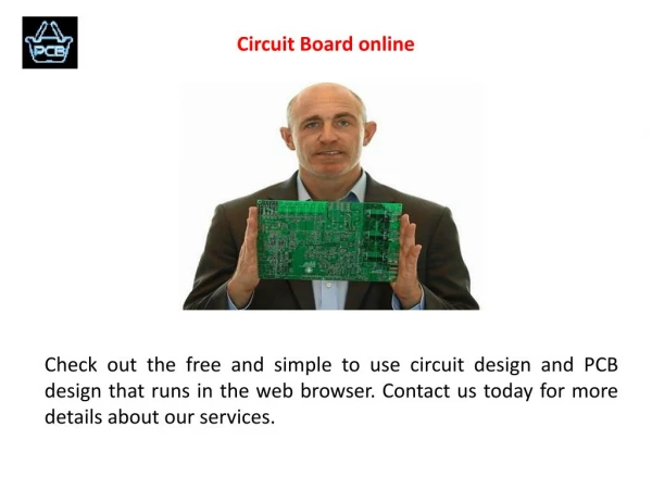
Visionics is an Electronic Circuit Design Software company in Sweden. Visionics is an electronic design automation software company in Sweden. Visionics is Electronic Design Software Company which design Circuit Board Components in Sweden. Visit http://www.visionics.a.se/

E N D
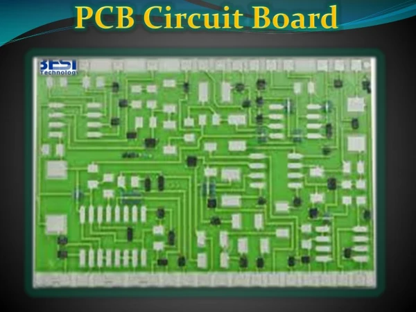
Introduction to PCB Layout Design Layout Editor is used to design the PCB layout of a circuit. The project database supports design of 32-layers boards (28 electrical layers, 2 silk-screen & 2 masks). The design can be captured either in schematic capture or directly in layout editor. In the former case, the design is front annotated to the layout editor and in the latter case it is back annotated to schematic editor. When front annotated to the Layout, all packaged components on the schematic will be positioned in the layout at board datum (0, 0). PCB Layout can also be designed without a pre-existing schematic. Components are automatically loaded as a result of packaging executed while editing the schematic diagram of the circuit. Layout may be started without schematic; In that case, new parts may be loaded on the board in similar fashion as in Schematic Editor. Location and orientation of components is defined either by manual relocation to desired position, using coordinates or with the help of auto placer. Traces may be routed manually with automatic via insertion whenever routing layer is changed. Sixteen types of user defined via pads are supported. Layout Editor also includes a number of online automatic functions to route/ reroute traces for single nets and to reroute existing traces for relocated components. Dedicated full board auto router and import /export interfaces are also integrated with PCB Layout Editor. Copper pour areas are defined as polygons and may be placed on any trace layer. Insertion of air gaps and thermal pads on artworks is automatic. Design rules for manual, semi-automatic and automatic routing of traces and component placement are user defined and may be set individually for each project. Design rules violation, clearance errors and missing or incomplete connections are detected automatically.
Configuring The Editor Board Configuration Default board formats for the workspace may be set in the Project Explorer | System | Options window. The user can select pre-defined formats or create own formats. It is advisable to set the required board size to avoid unnecessary wastage of space. Features Maximum board size available - 4m x 4m. Maximum number of layers on board – 32 (28 trace layers, 2 silk screen & 2 masks) Available page formats – American & European. American formats: AA , AB , AC , AD , AE , AFEuropean formats: EA , EB , EC, ED , EE , EFBy default American format AA is enabled.
Steps To Follow To Define Board Outline • Select Board Format from Tools toolbar. • Select the function tool Define Outline. • The option tool Create Board will be enabled. This tool enables free hand drawing, using which a board of desired shape can be drawn on the workspace. • To select a pre-defined board format, select the option tool extual Mode. The Properties Board Outline (Create) dialog pops up as shown in Fig. • Enter the desired values and click ACCEPT button.
Loading components This section deals with how to extract components from the respective libraries and position them on the layout editor. The components placed on the schematic, which contain both symbol and package, are front annotated to the layout after packing. These components are positioned at board datum (0, 0) automatically and can be relocated either manually or automatically. If new parts are required to be added, they may be extracted as part using options of the function tool Open part library. Only parts that contain both symbol and package will be automatically back annotated to the schematic. Components can be loaded in the working area using any one of the following three ways:\ Component Browser ii. Using Library Explorer iii. Using Library Browser iv. Add Components Select Open part library function tool to display the last three option tools.
Contact Us VisionicsEurope VisionicsSweden HB GaNorrtaljev 97, 182 47 Enebyberg.Sweden.Tel : +46 8 792 2620.Fax: +46 8 758 7869.E-mail: visionics@bredband.net Visionics India Visionics India Pvt. Ltd.,Technopark, Trivandrum - 695 581.Kerala. Tel : +91 471 2700673.Fax: +91 471 2700673.E-mail: viplasia@visionicsasia.net Customer Support and Salessales@visionics.a.se Visionics Support DeskE-mail: support@visionics.a.se