Download
1 / 33
330 likes | 500 Views
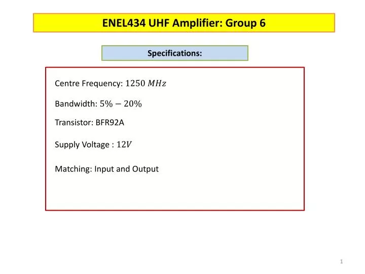
ENEL434 UHF Amplifier: Group 6. Specifications:. Centre Frequency:. Bandwidth:. Transistor: BFR92A. Supply Voltage :. Matching: Input and Output. DC Biasing of the Transistor. The transistor datasheet below shows that there is no need to exceed.

E N D
ENEL434 UHF Amplifier: Group 6 Specifications: Centre Frequency: Bandwidth: Transistor: BFR92A Supply Voltage : Matching: Input and Output
DC Biasing of the Transistor The transistor datasheet below shows that there is no need to exceed . In order to obtain emitter degeneration an value of was chosen. A voltage of half the of 12V was chosen, so This then allows to be calculated by can be found by Chosen as larger
DC Biasing of the Transistor- Continued • The Thevenin equivalent circuit could then be constructed in order to calculate the values of RB1 and RB2. • We want be less than in order to have independent from Where was chosen as is defined as Rearrange Substitute
Constructing Transistor Model in MWO The value of was changed in order to obtain the desired bias conditions by using the transistor circuit in Microwave office. Values for all the connection pad sizes were provided in the initial MWO file given. A series parasitic inductance in the capacitor was also included, this value was 1nF from the capacitor datasheet. Transistor Circuit
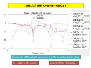
Finding S Parameters of Amplifier Plotting the S parameters from the Amplifier Schematic. 1.25GHz Giving the Values
The S parameters were then used to calculate the values = Using Conjugate matching
Testing Ideal TLs In Microwave Office These values are similar to the values expected from previous slides Source Load
Testing TLs With loads • Checking the conjugate matching calculations are correct • Expecting a minor error due to graphical method used to obtain results These values are similar to those calculated so the design can now be put into a microstrip implementation
Testing TLs with transistor bias Bandwidth of 0.175GHz This shows that the amplifier operates well around the 1.25GHz operating frequency.
Replacing ideal Transmission lines with Microstrips The values for the width and length were calculated using the TXline function in MWO Source Load W = 3.07mm d = 19.46 mm d = 16.04 mm l = 9.37 mm l = 39.37 mm
Replacing ideal Transmission lines with Microstrips This shows a little deviation of the intended reflection values
Adding a T intersection to the Model T intersections were placed in the schematic to mimic the actual circuit. The length of the microstrips was decreased by 1.5mm as the T intersection are 3mm in width. The 5mm strip on the end is added as a contact for the decoupling capacitors
Fine Tuning the T intersection Model The lengths were fine tuned in order to bring the reflection coefficient values back to the desired conjugate values.
AMP test of Microstrip This shows that the amplifier still works with microstrip line implementation of the transmission line networks. The gain is now lower due to copper losses
Full Circuit Test Now inserting all of the components into the circuit The capacitor values were chosen by trial using MWO simulation results in order to gain a desirable frequency response. as well as the
Initial Frequency Response. This is not nearly as nice as expected. Stub capacitors should be checked as well as input and output capacitors.
Shorting Stub Capacitors Bypassing via circuitry and parasitic inductance. This shows that it is the stub capacitor connections causing problems
Smith Chart of Stub Connections 330pF Not a SC at the centre frequency Changing the capacitor values to 8.2pF causes the capacitor to act as a SC. Could still have a better frequency response.
Parallel Capacitance Two capacitors can be placed in parallel in order to gain a better frequency response. This however has made it worse at this stage.
Parallel Capacitance + Resistor A resistor is placed in series with the large capacitor in order to negate the effect of parallel resonance in the circuit. The resistor value was chosen to be in order to gain the short circuit curve shown on the right.
Circuit Response with Parallel Capacitors This shows how the circuit is again working properly
Circuit including Microstrips This shows the response of a circuit with microstrip components in the stubs.
Final Circuit Output Network Transistor Input Network DC biasing Network The final circuit was then created and has been broken down into readable sections
Final DC Bias Circuit Used a decoupling capacitor, assumed 100nF of parasitic inductance. This is in parallel with a 330pF for high frequency rejection.
Final Frequency Response Bandwidth This was also tried with a series power source inductance of to mimic a large inductance in the line. The results were very similar. The circuit now meets all of the requirements and can be laid out.
Currents at Ports Peaks around operating Frequency This shows that the DC components of the ports are filtered, also the RF component into the DC source is low but still present. This could be filtered by additional EMI filters.
Creating Layout The stub line on the input and the transmission line on the output were bent in order to conserve space. - These bends were taken into account in previous graphs The DC lines could be changed as needed without the issue of affecting the response.
PCB Layout This is the final PCB design to be used for the assignment. This was created by exporting the design in Coral Draw. Tracks = Black Vias = White