Download
1 / 16
160 likes | 425 Views
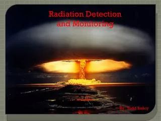
"Radiation Tolerant and Intelligent Memory for Space“ T. Dargnies 1 , J. Herath 2 , T. Ng 2 , C. Val 1 , J.F. Goupy 1 , and J.P. David 3 1 3D PLUS 2 NASA Langley Research Center 3 ONERA 2005 MAPLD International Conference September 7-9, 2005 Washington DC. Contents Introduction

E N D
"Radiation Tolerant and Intelligent Memory for Space“ T. Dargnies1, J. Herath2, T. Ng2, C. Val1, J.F. Goupy1, and J.P. David3 1 3D PLUS2 NASA Langley Research Center 3 ONERA 2005 MAPLD International Conference September 7-9, 2005 Washington DC
Contents • Introduction • Preliminary design / heritage / radiation assessment • Radiation testing / radiation results • 3.1 FPGA Radiation results • 3.2 SDRAM Radiation results • 3.3 Voltage regulator results • Design completion • Prototypes results / functional validation • Conclusion • Authors information
Introduction • In space applications such as earth observation or scientific missions, data storage requirements are always increasing. Moreover, environmental and radiation stress on electronics in space is very harsh. 3D PLUS, whose assembly process is certified by ESA and NASA has designed and manufactured for several years many modules (memory based, CPU, converters) for space applications. • In partnership with NASA Langley Research Center under NASA Contract NAS1-0364, 3D PLUS developed the first high density and fast access time memory module tolerant of space radiation effects. This brand-new module operates like a simple SRAM (Addresses / Data / Control signals), and has a maximum capacity of 3Gb. • Radiation requirements of this SRAM-like module are: • ü TID tolerant up to 100 krad(Si) (reference chosen orbit is Geosynchronous / duration is 15 years) • ü Single Event Effects immunity up to 60 MeV/mg.cm² (Latchup and Upsets) • To manage TID and SEE radiation effects on electronics, specific hardware and software protections are embedded in order to respect previous requirements. This module decreases design complexity for space based boards requiring memory with its simple interface and internal radiation tolerance management (shielding, EDAC, over current protections,…). The first prototypes have been manufactured and tested by 3D PLUS in April 2005, first flight parts will be launched in 2006 or 2007.. • This module is to be directly connected to a processor or equivalent and considered as a radiation tolerant device. • ACRONYMS: CPU = Central Processing Unit, EDAC System = Error Detection And Correction System, ESA = European Space Agency, FPGA = Field Programmable Gate Array, MEU = Multiple Event Upset, S(D)RAM = Synchronous (Dynamic) Random Access Memory,SEE = Single Event Effects, SEFI = Single Event Functional Interrupt, SEL = Single Event Latchup, SET = Single Event Transient, SEU = Single Event Upset, TID = Total Ionizing Dose
VCC Linear Regulator 512 Mb SDRAM GND 512 Mb SDRAM Ctrl +@ Interface and SDRAM controller FPGA 8 48 (data bus) 512 Mb SDRAM 8 8 8 8 8 D_In 512 Mb SDRAM D_Out 512 Mb SDRAM 50 Mhz Configuration PROM 512 Mb SDRAM 2. Preliminary design / heritage / radiation assessment Previous 3D PLUS memory modules for space applications have embedded ELPIDA (former HITACHI) SDRAMs. In fact, 3D PLUS has a long history and significant experience with the 512 Mb monolithic die EDS5108ABTA which has been fully characterized versus TID (CO60 TID characterization) and SEE. This experience and knowledge is why this particular memory was chosen as the basis for this design. Simplified schematic of the module Note1: Each active component is also protected with a specific thermal shutdown (over current protection) component. Note2: Internal CLK = 100 MHz (SDRAM operation). Note3: All components and signals are not represented in this simplified schematic.
To ensure that the proposed design would meet or exceed the radiation requirements, the radiation characteristics of all active components on the bill of materials were analysed. Radiations effects on components were considered in 3 steps: • Step 1: Latchup events = If component is not latchup immune with LET < 60 MeV/mg.cm² component will not be used. If immune, with LET > 60 MeV/mg.cm² component may be chosen. • Step 2: Total Ionizing Dose = Depending on components TID tolerance, specific shielding (tantalum, 3D PLUS FP4450 resin) will be considered. • Step 3: Other events (SEU/MEU/SET) = Depending on components tolerance, design will be adapted and specific software will be embedded.
3. Radiation testing & radiation results • To ensure that requirements are respected, several radiation testing have been performed TID on all active components: • SEL on VIRTEX II FPGA, SDRAM memories and voltage regulator (Eeprom memory purchased in space quality level) • SEU/MEU/SEFI on SDRAM memories • SET on Linear regulator • Sum up the of radiation results Note:1 Test performed by ONERA at Toulouse (France), 2 Test performed by RAD at TAMU (USA), 3 Test performed by 3D PLUS at TAMU (USA)
Let’s focus on the three main and critical components tested under radiation effects (EEPROM radiation characteristics are guaranteed by Xilinx Datasheet because purchased in space quality level. 3.1 Xilinx XQ2V1000 FPGA Radiation results / SEL Testing SEL Testing at Texas A&M University The Xilinx FPGA showed no SEL events at LETs of 86.6MeV-cm2/mg (normal incidence irradiation) and at 124MeV-cm2/mg (effective LET at 45-degrees angle of incidence irradiation). Each irradiation was performed to a total effective fluence of 1E7ions/cm2).
3.2.1 ELPIDA EDS5108ABTA SDRAM Radiation results (TID) CO60 TID Testing up to 50Krad(Si) Conclusion: SDRAM is within specifications at 50 Krad(Si)
3.2.2 SDRAM Radiation results (SEL / SEU / SEFI) Heavy Ions Testing up to 74 MeV/mg.cm² SEL X-Section as a function of LET In addition, the SDRAM memories showed no SEL events at LETs of 40, 60, and 80MeV-cm2/mg at a temperature of 85ºC. Test was performed at higher temperatures and the parts showed no SEL events at a LET of 80MeV-cm2/mg at temperatures of 85, 100 and 125ºC.
3.3.1 Voltage Regulator Radiation results (TID) CO60 TID Testing up to 15Krad(Si) Conclusion: Voltage Regulator is within specifications at 10 krad (Si)
3.3.2 Voltage Regulator Radiation results (SEL / SET) Heavy Ions Testing up to 60 MeV/mg.cm² SEE Testing conclusion: This component show Single Event phenomenon at LET of 86.6 MeV.cm²/mg and ambient temperature. A high internal current is observed after an unexpected shutdown of the output voltage of the part.This unexpected shutdown of the regulator may be the consequence of the impact of ions on the digital part of the die that embed the automatic thermal shutdown and other electronics. No SEL is observed at both LET of 60 MeV.cm²/mg and 86.6 MeV.cm²/mg, however, at these LET, Single Event Transients are observed on the output voltage .
4. Design completion • Based on these radiation test results, we were able to use for each radiation phenomenon specific design rules. • · 1:Latchup events: No Latchup events were detected on any of the tested parts. This bill of material will fit the SELth > 60 MeV/mg.cm² requirement. • For system safety, thermal shutdown protection is provided to every active part (memories, FPGA, regulator). • · 2: Other events (SEU / MEU / SEFI /SET): • SEU/MEU/SEFI on FPGA: Triple Modular Redundancy and scrubbing is used to mitigate upsets in the FPGA. • SEU/MEU/SEFI on SDRAM : The FPGA interfaces with the 6 SDRAMs in two possible modes: • Triple redundancy (same data on 3 banks/16 bits). Full module data storage size is 1 Gb. • EDAC system. Two banks are used for data storage. Full module data storage size is 2 Gb • SET on voltage Regulator: During Latchup testing, at a LET of 60 MeV/mg.cm² (fluence of 1E+7 ions/cm²), some Single Event Transients were observed on the output voltage of the regulator. Additional embedded energy capacitors of 940 uF were added to compensate for these voltage transients. • · 3: Total Ionizing Dose: TID tolerance is different from one active component to another. • For TID, a Geosynchronous orbit and a mission duration of 15 years was chosen. With these parameters, OMERE simulation software provides us the associated curve of TID versus Al thickness (see figure 1).
Figure 1 : Dose Vs Al thickness for Geosynchronous orbit TID requirement is 100 Krad(Si). Based on Figure 1 simulation results and components testing TID results, we added specific shielding on components. Epoxy resin HYSOL FP4450 (density = 1.77 g/cm3) is the moulding resin used by 3D PLUS. With AutoCAD software and design file of the module, minimum thickness of epoxy resin around a component in X, Y and Z axis is calculated. When required extra Tantalum (density = 16.6 g/cm3) shielding is added on parts.To manage the TID requirement, we added 250 µm of Tantalum on all the active parts (3 axis protection) except for TPS75715 and MAX803 components (750 µm). Three dimensional calculations performed by 3D PLUS for each active component permits to conclude that 100 krad(Si) requirement for a Geosynchronous Orbit and a mission duration.
Picture 2: After final shielding (top) Picture 1: Before final shielding (top) Prototypes have been manufactured and tested in April 2005. First results are very promising (see pictures 1, 2 & 3). The part electronically behaves as planned. Embedded software (VHDL written for test), permits simulation of SDRAM Single Event Upsets to check that the mitigation system operates as intended. Picture 3: After final shielding (bottom) 5. Prototypes results / functional validation
6. Conclusion 3D PLUS, in partnership with NASA LaRC, designed and manufactured the first high density and fast access time SRAM-like memory module (1Gb or 2Gb available) TID tolerant to 100 krad (Si) and SEE immune up to 60 MeV/mg.cm². The real improvement of this brand-new memory is the significantly reduced board design time (no complex controller, no SEU management, no TID management required anymore). This module is to be directly connected to a processor or equivalent and considered as a radiation tolerant device. Related paper: Presentation of Tak-kwong Ng and Jeffrey Herath of NASA LARC on hardware and software design of this module (A208).
7. Author Information Corresponding (and Presenting) Author: Timothée Dargnies, 3D PLUS, 641 rue H. Boucher 78532 Buc (France), phone : +33 1 30 83 26 56, fax: +33 1 39 56 25 89, email: tdargnies@3d-plus.com Contributing Authors: Jeff Herath, NASA LaRC, Mail Stop 488, Hampton VA23681 (USA), phone : +1 757 864 1098, email : jeffrey.a.herath@nasa.gov Tak-kwong Ng, NASA LaRC, Mail Stop 488, Hampton VA23681 (USA), phone : +1 757 864 1097, email : t.ng@nasa.gov Christian Val, 3D PLUS, 641 rue H. Boucher 78532 Buc (France), phone : +33 1 30 83 26 51, fax: +33 1 39 56 25 89, email: cval@3d-plus.com Jean Francois Goupy, 3D PLUS, 641 rue H. Boucher 78532 Buc (France), phone : +33 1 30 83 26 53, fax: +33 1 39 56 25 89, email: jfgoupy@3d-plus.com Jean-Pierre David, ONERA, Complexe scientifique 2 avenue E. Belin, 31055 Toulouse Cedex (France), phone : + 33 5 62 25 27 37, email : jean-pierre.david@onecert.fr