Download
1 / 48
510 likes | 781 Views
Basic Logic Design with Verilog. TA: Chen-han Tsai. Outline. Introduction to HDL/ Verilog Gate Level Modeling Behavioral Level Modeling Test bench Summary and Notes Simulation using Silos. Introduction to HDL/ Verilog. What is HDL/Verilog. Why use HDL (Hardware Description Language)?

E N D
Basic Logic Designwith Verilog TA: Chen-han Tsai
Outline • Introduction to HDL/ Verilog • Gate Level Modeling • Behavioral Level Modeling • Test bench • Summary and Notes • Simulation using Silos
What is HDL/Verilog • Why use HDL (Hardware Description Language)? • HDL ←→ layout by human • Reduce cost and time • Verilog is one of the most popular HDLs • VHDL (another popular HDL) • Key features of Verilog • Supports Various levels • Behavior level (Register Transfer Level, RTL) • Gate level • Switch level • Simulate design functions
Verilog Hardware Design Flow
in1 a1 a1_o out iv_sel o1 in2 a2 a2_o n1 sel iv_sel Gate Level Description Gate Level:you see only gates and wires in the code
Behavioral Level Description assign always block RTL:you may see high level behavior in the code
module name in/out port declaration syntax port/wire declaration kernel hardware gate-connection/ behavior A Simple Verilog Code
Module • Basic building block in Verilog. • Module • Created by “declaration” (can’tbe nested) • Used by “instantiation“ • Interface is defined by ports • May contain instances of other modules • All modules run concurrently
Module Instantiation instance example
Port Connection • Connect module port by order list • FA1 fa1(c_o, sum, a, b, c_i); • Not fully connected • FA1 fa3(c_o,, a, b, c_i); • Connect module port by name • FA1 fa2(.A(a), .B(b), .CO(c_o),.CI(c_i), .S(sum)); • Recommended
Verilog Language Rule • Case sensitive • Identifiers: • Digits 1…9 • Underscore_ • Upper and lower case letters from the alphabet • Terminate line with semicolon “;” • Comments: • Single line: // it’s a single line comment example • Multiline: /* when the comment exceeds single line, multiline comment is necessary*/
Register and Net • Registers • Keyword : reg, integer, time, real • Storage element • Assignment in “always” block • Nets • Keyword : wire, wand, wor, tri triand, trior, supply0, supply1 • Doesn’t store value, just a connection • input, output, inout are default “wire” • Can’t appear in “always” block assignment
Value and Number expressions • Verilog value set consists of four basic values: • 0 represent a logic zero or false condition • 1 represent a logic one or true condition • x represent an unknown logic value • z represent a high-impedance stage
Value and Number Expressions : Examples 659 // unsized decimal ‘h 837ff // unsized hexadecimal ‘o7460 // unsized octal 4af // illegal syntax 4’b1001 // 4-bit binary 5’D 3 // 5-bit decimal 3’b01x // 3-bit number with unknown LSB 12’hx // 12-bit unknown 8’d -6 // illegal syntax -8’d 6 // phrase as - (8’d6) // underline usage 27_195_000 16’b0001_0101_0001_1111 32’h12ab_f001 // X and Z is sign-extended reg [11:0] a; initial begin a = ‘hx; // yields xxx a = ‘h3x; // yields 03x a = ‘h0x; // yields 00x end
Module B Module A Module C 3‘o7 Net Concatenations : An Easy Way to Group Nets Representations Meanings {b[3:0],c[2:0]} {b[3] ,b[2] ,b[1] ,b[0], c[2] ,c[1] ,c[0]} {a,b[3:0],w,3’b101} {a,b[3] ,b[2] ,b[1] ,b[0],w,1’b1,1’b0,1’b1} {4{w}} {w,w,w,w} {b,{3{a,b}}} {b,a,b,a,b,a,b}
Compiler Directives • `define • `define RAM_SIZE 16 • Defining a name and gives a constant value to it. • `include • `include adder.v • Including the entire contents of other verilog source file. • `timescale • `timescale 100ns/1ns • Setting the reference time unit and time precision of your simulation. • Only 1, 10, and 100 are legal values.
System Tasks • $monitor • $monitor ($time,"%d %d %d",address,sinout,cosout); • Displays the values of the argument list whenever any of the arguments change except $time. • $display • $display ("%d %d %d",address,sinout,cosout); • Prints out the current values of the signals in the argument list • $finish • $finish • Terminate the simulation
Gate Level Modeling Gate Level Modeling Primitives Case Study
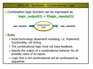
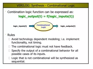
Gate Level Modeling • Steps • Design the smallest sub-modules • Construct modules with built sub-modules • Connections • Use “assign a = b;” to connect a and b (a is driven by b) • HDL: Hardware Description Language • Architecture figure first, then start to write code!!
Primitives • Primitives are modules ready to be instanced • Verilog build-in primitive gate • not, buf • and, or, not, buf, xor, nand, nor, xnor • Design ware • Vender-provided primitive gates • User-built primitive gate • Your building block modules (sub-modules)
Case Study1-bit Full Adder • Co = (A‧B‧Ci’)+(A‧B’‧Ci)+(A’‧B‧Ci)+(A‧B‧Ci) = (A‧B‧Ci’)+(A‧B’‧Ci)+ (B‧Ci) = { A‧[ (B‧Ci’)+(B’‧Ci) ] } + (B‧Ci)
Case Study1-bit Full Adder • S = (A’‧B’‧Ci)+(A’‧B‧Ci’)+(A‧B’‧Ci’)+(A‧B‧Ci) = { A’‧[ (B’‧Ci)+(B‧Ci’) ] } + { A‧[ (B’‧Ci’)+(B‧Ci) ] }
Case Study1-bit Full Adder • Design hierarchy
Case Study1-bit Full Adder • Basic gate: 1-bit AND
Case Study1-bit Full Adder • Basic gate: 1-bit OR
Case Study1-bit Full Adder • Connect co • Instance AND, OR gates
Case Study1-bit Full Adder • Connect s • Instance AND, OR gates
Case Study1-bit Full Adder • Full Adder Connection • Instance co, s
Case Study1-bit Full Adder • Code
Behavioral Level Modeling Behavioral Level Modeling Case Study
Behavioral Level Modeling • High level description • User friendly • Concise code • Widely used for some common operations • +,-,* • &,|,~ • Two main formats • always block • assign
Case Study1-bit Full Adder LHS signals in always block should be declared as “reg”
Summary • Design module • Gate level or behavior level • Real hardware • Modules exists all the time • Each module has architecture figure • Plot architecture figures before you write verilog codes • Test bench • Feed input data and compare output values versus time • Usually behavior level • Not real hardware, just like C/C++
Note • Verilog is a platform • Support hardware design (design module) • Also support C/C++ like coding (test bench) • How to write verilog well • Know basic concepts and syntax • Get a good reference (a person or some code files) • Form a good coding habit • Naming rule, comments, format partition (assign or always block) • Hardware • Combinational circuits (today’s topic) • 畫圖(architecture), then 連連看(coding) • Sequential circuits (next topic) • register: element to store data
Create new project • Write your verilog design code • Create a new project: • Project -> New -> (enter your project name) • Include your verilog file(s) • (choose your .v file) -> (click Add bottom) -> (click OK) • Note that testbench should be included • Then run and debug
Run and Debug • Run • Press F5 or click the “GO” icon on tool bar • An output window is generated to show whether there exists errors. • Debug • Press “open analyzer” on the toolbar • Press “open explorer” on the toolbar • Choose signals you want to watch • Click right button and select “Add signal to analyzer” • Then you can debug with waveform