Download
1 / 76
831 likes | 1.93k Views
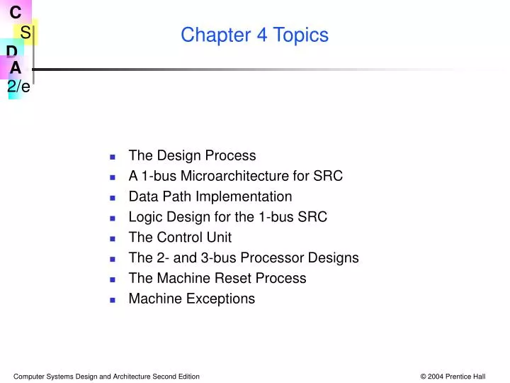
Chapter 4 Topics. The Design Process A 1-bus Microarchitecture for SRC Data Path Implementation Logic Design for the 1-bus SRC The Control Unit The 2- and 3-bus Processor Designs The Machine Reset Process Machine Exceptions. Abstract and Concrete Register Transfer Descriptions.

E N D
Chapter 4 Topics • The Design Process • A 1-bus Microarchitecture for SRC • Data Path Implementation • Logic Design for the 1-bus SRC • The Control Unit • The 2- and 3-bus Processor Designs • The Machine Reset Process • Machine Exceptions
Abstract and Concrete Register Transfer Descriptions • The abstract RTN for SRC in Chapter 2 defines “what,” not “how” • A concrete RTN uses a specific set of real registers and buses to accomplish the effect of an abstract RTN statement • Several concrete RTNs could implement the same ISA
A Note on the Design Process • In this chapter presents several SRC designs • We started in Chap. 2 with an informal description • In this chapter we will propose several block diagram architectures to support the abstract RTN, then we will: • Write concrete RTN steps consistent with the architecture • Keep track of demands made by concrete RTN on the hardware • Design data path hardware and identify needed control signals • Design a control unit to generate control signals
EA 12 Fig. 4.2 High-Level View of the 1-Bus SRC Design ADD SUB AND OR SHR SHRA SHL SHC NOT NEG C=B INC4
Constraints Imposed by the Microarchitecture • One bus connecting most registers allows many different RTs, but only one at a time • Memory address must be copied into MA by CPU • Memory data written from or read into MD • First ALU operand always in A, result goes to C • Second ALU operand always comes from bus • Information only goes into IR and MA from bus • A decoder (not shown) interprets contents of IR • MA supplies address to memory, not to CPU bus
Tbl 4.1 Concrete RTN for add: Step RTN T0. MAPC: C PC + 4; T1. MD M[MA]: PC C; T2. IR MD; T3. A R[rb]; T4. C A + R[rc]; T5. R[ra] C; IF IEx. Abstract and Concrete RTN for SRC add Instruction Abstract RTN: (IR M[PC]: PC PC + 4; instruction_execution); instruction_execution := ( • • • add (:= op= 12) R[ra] R[rb] + R[rc]: • Parts of 2 RTs (IR M[PC]: PC PC + 4;) done in T0 • Single add RT takes 3 concrete RTs (T3, T4, T5)
Concrete RTN Gives Information about Sub-units • The ALU must be able to add two 32-bit values • ALU must also be able to increment B input by 4 • Memory read must use address from MA and return data to MD • Two RTs separated by : in the concrete RTN, as in T0 and T1, are operations at the same clock • Steps T0, T1, and T2 constitute instruction fetch, and will be the same for all instructions • With this implementation, fetch and execute of the add instruction takes 6 clock cycles
Concrete RTN for Arithmetic Instructions: addi Abstract RTN: • Differs from add only in step T4 • Establishes requirement for sign extend hardware addi (:= op= 13) R[ra] R[rb] + c216..0 {2's comp. sign extend} : Tbl 4.2 Concrete RTN for addi: Step RTN T0. MAPC: C PC + 4; T1. MD M[MA]; PC C; T2. IR MD; T3. A R[rb]; T4. C A + c216..0 {sign ext.}; T5. R[ra] C;
Fig. 4.3 More Complete view of Registers and Buses in 1-bus SRC Design—Including Some Control Signals • Concrete RTN lets us add detail to the data path • Instruction register logic & new paths • Condition bit flip-flop • Shift count register Keep this slide in mind as we discuss concrete RTN of instructions.
Abstract and Concrete RTN for Load and Store • ld (:= op= 1) R[ra] M[disp] : • st (:= op= 3) M[disp] R[ra] : • where • disp31..0 := ((rb=0) c216..0 {sign ext.} : • (rb0) R[rb] + c216..0 {sign extend, 2's comp.} ) : Tbl 4.3 Step RTN for ld RTN for st T0-T2 Instruction fetch T3. A (rb=0 0: rb0 R[rb]); T4. C A + (16@IR16#IR15..0); T5. MA C; T6. MD M[MA]; MD R[ra]; T7. R[ra] MD; M[MA] MD;
Notes for Load and Store RTN • Steps T0 through T2 are the same as for add and addi, and for all instructions • In addition, steps T3 through T5 are the same for ld and st, because they calculate disp • A way is needed to use 0 for R[rb] when rb=0 • 15 bit sign extension is needed for IR16..0 • Memory read into MD occurs at T6 of ld • Write of MD into memory occurs at T7 of st
Concrete RTN for Conditional Branch br (:= op= 8) (cond PC R[rb]): cond := ( c32..0=0 0: never c32..0=1 1: always c32..0=2 R[rc]=0: if register is zero c32..0=3 R[rc]0: if register is nonzero c32..0=4 R[rc]31=0: if positive or zero c32..0=5 R[rc]31=1 ): if negative Tbl 4.4 Step Concrete RTN T0-T2 Instruction fetch T3. CON cond(R[rc]); T4. CON PC R[rb];
Notes on Conditional Branch RTN • c32..0are just the low order 3 bits of IR • cond() is evaluated by a combinational logic circuit having inputs from R[rc] and c32..0 • The one bit register CON is not accessible to the programmer and only holds the output of the combinational logic for the condition • If the branch succeeds, the program counter is replaced by the contents of a general reg.
Tbl 4.5 Step Concrete RTN T0-T2 Instruction fetch T3. n IR4..0; T4. (n=0) (n R[rc]4..0 C R[rb]; T6. Shr (:= (n≠0) (C31..0 0#C31..1n n-1; Shr) ); T7. R[ra] C; step T6 is repeated n times Abstract and Concrete RTN for SRC Shift Right shr (:= op = 26) R[ra]31..0 (n @ 0) # R[rb]31..n : n := ( (c34..0=0) R[rc]4..0 : shift count in reg. (c34..0≠0) c34..0 ): or const. field
Notes on SRC Shift RTN • In the abstract RTN, n is defined with := • In the concrete RTN, it is a physical register • n not only holds the shift count but is used as a counter in step T6 • Step T6 is repeated n times as shown by the recursion in the RTN • The control for such repeated steps will be treated later
Data Path/Control Unit Separation • Interface between data path and control consists of gate and strobe signals • A gate selects one of several values to apply to a common point, say a bus • A strobe changes the values of the flip-flops in a register to match new inputs • The type of flip-flop used in regs. has much influence on control and some on data path • Latch: simpler hardware, but more complex timing • Edge triggering: simpler timing, but about 2 hardware
Reminder on Latch and Edge-Triggered Operation • Latch output follows input while strobe is high D D Q C C Q • Edge triggering samples input at edge time D D Q C C Q
Fig. 4.4 The SRC Register File and Its Control Signals • Rout gates selected reg. onto bus • Rin strobed selected reg. from bus • BAout differs from Rout by gating 0 when R[0] is selected BA = Base Address
Fig. 4.4 The SRC Register File and Its Control Signals A ((rb=0) 0: (rb!=0) R[rb]); Recall T3, what control signals would need to be asserted to carry out this step
Fig. 4.5 Extracting c1, c2, and op from the Instruction Register • I21 is the sign bit of C1 that must be extended • I16 is the sign bit of C2 that must be extended • Sign bits are fanned out from one to several bits and gated to bus
Fig. 4.6 CPU to Memory Interface: MA and MD Registers • MD is loaded from memory bus or from CPU bus • MD can drive CPU bus or memory bus
Figure 4.8. A Logic-Level Design for One Bit of the 1-Bus SRC ALU
From Concrete RTN to Control Signals: The Control Sequence Tbl 4.6—The Instruction Fetch • The register transfers are the concrete RTN • The control signals that cause the register transfers make up the control sequence • Wait prevents the control from advancing to step T3 until the memory asserts Done Step Concrete RTN Control Sequence T0. MA PC: C PC+4; PCout, MAin, Inc4, Cin T1. MD M[MA]: PC C; Read, Cout, PCin, Wait T2. IR MD; MDout, IRin T3. Instruction_execution
Control Steps, Control Signals, and Timing • Within a given time step, the order in which control signals are written is irrelevant • In step T0, Cin, Inc4, MAin, PCout == PCout, MAin, Inc4, Cin • The only timing distinction within a step is between gates and strobes • The memory read should be started as early as possible to reduce the wait • MA must have the right value before being used for the read • Depending on memory timing, Read could be in T0
Control Sequence for the SRC add Instruction add (:= op= 12) R[ra] R[rb] + R[rc]: Tbl 4.7 The Add Instruction • Note the use of Gra, Grb, & Grc to gate the correct 5 bit register select code to the regs. • End signals the control to start over at step T0 Step Concrete RTN Control Sequence T0. MA PC: C PC+4; PCout, MAin, Inc4, Cin, Read T1. MD M[MA]: PC C; Cout, PCin, Wait T2. IR MD; MDout, IRin T3. A R[rb]; Grb, Rout, Ain T4. C A + R[rc]; Grc, Rout, ADD, Cin T5. R[ra] C; Cout, Gra, Rin, End
Control Sequence for the SRC addi Instruction addi (:= op= 13) R[ra] R[rb] + c216..0 {2's comp., sign ext.} : • The c2out signal sign extends IR16..0 and gates it to the bus Tbl 4.8 The addi Instruction Step Concrete RTN Control Sequence T0. MA PC: C PC + 4; PCout, MAin, Inc4, Cin, Read T1. MD M[MA]; PC C; Cout, PCin, Wait T2. IR MD; MDout, IRin T3. A R[rb]; Grb, Rout, Ain T4. C A + c216..0 {sign ext.}; c2out, ADD, Cin T5. R[ra] C; Cout, Gra, Rin, End
Step Concrete RTN Control Sequence T0-T2 Instruction fetch Instruction fetch T3. A (rb=0) 0: rb0 R[rb]; Grb, BAout, Ain T4. C A + c216..0 {sign ext.}; c2out, ADD, Cin T5. MA C; Cout, MAin T6. MD R[ra]; Gra, Rout, MDin, Write T7. M[MA] MD; Wait, End } address arithmetic Control Sequence for the SRC st Instruction • st (:= op= 3) M[disp] R[ra] : • disp31..0 := ((rb=0) c216..0 {sign ext.} : • (rb0) R[rb] + c216..0 {sign extend, 2's comp.} ) : • Note BAout in T3 compared to Rout in T3 of addi The st Instruction
Fig. 4.9 The Shift Counter • The concrete RTN for shr relies upon a 5 bit register to hold the shift count • It must load, decrement, and have an = 0 test
Tbl 4.10 Control Sequence for the SRC shr Instruction—Looping • Step Concrete RTN Control Sequence • T0-T2 Instruction fetch Instruction fetch • T3. n IR4..0; c1out, Ld • T4. (n=0) (n R[rc]4..0); n=0 (Grc, Rout, Ld) • T5. C R[rb]; Grb, Rout, C=B, Cin • T6. Shr (:= (n≠0) n0 (Cout, SHR, Cin, • (C31..0 0#C31..1: Decr, Goto6) • n n-1; Shr) ); • T7. R[ra] C; Cout, Gra, Rin, End • Conditional control signals and repeating a control step are new concepts
Branching cond := ( c32..0=0 0: c32..0=1 1: c32..0=2 R[rc]=0: c32..0=3 R[rc]0: c32..0=4 R[rc]31=0: c32..0=5 R[rc]31=1 ): • This is equivalent to the logic expression cond = (c32..0=1) (c32..0=2)(R[rc]=0) (c32..0=3)(R[rc]=0) (c32..0=4)R[rc]31 (c32..0=5)R[rc]31
Fig. 4.10 Computation of the Conditional Value CON • NOR gate does =0 test of R[rc] on bus
Tbl 4.11 Control Sequence for SRC Branch Instruction, br br (:= op= 8) (cond PC R[rb]): • Condition logic is always connected to CON, so R[rc] only needs to be put on bus in T3 • Only PCin is conditional in T4 since gating R[rb] to bus makes no difference if it is not used Step Concrete RTN Control Sequence T0-T2 Instruction fetch Instruction fetch T3. CON cond(R[rc]); Grc, Rout, CONin T4. CON PC R[rb]; Grb, Rout, CON PCin, End
Summary of the Design Process Informal description formal RTN description block diagram arch. concrete RTN steps hardware design of blocks control sequences control unit and timing • At each level, more decisions must be made • These decisions refine the design • Also place requirements on hardware still to be designed • The nice one way process above has circularity • Decisions at later stages cause changes in earlier ones • Happens less in a text than in reality because • Can be fixed on re-reading • Confusing to first time student
Fig. 4.11 Clocking the Data Path: Register Transfer Timing • tR2valid is the period from begin of gate signal till inputs to R2 are valid • tcomb is delay through combinational logic, such as ALU or cond logic
Signal Timing on the Data Path • Several delays occur in getting data from R1 to R2 • Gate delay through the 3-state bus driver—tg • Worst case propagation delay on bus—tbp • Delay through any logic, such as ALU—tcomb • Set up time for data to affect state of R2—tsu • Data can be strobed into R2 after this time tR2valid = tg + tbp + tcomb + tsu • Diagram shows strobe signal in the form for a latch. It must be high for a minimum time—tw • There is a hold time, th, for data after strobe ends
Effect of Signal Timing on Minimum Clock Cycle • A total latch propagation delay is the sum Tl = tsu + tw + th • All above times are specified for latch • th may be very small or zero • The minimum clock period is determined by finding longest path from ff output to ff input • This is usually a path through the ALU • Conditional signals add a little gate delay • Using this path, the minimum clock period is tmin = tg + tbp + tcomb + tl
Latches Versus Edge Triggered or Master Slave Flip-Flops • During the high part of a strobe a latch changes its output • If this output can affect its input, an error can occur • This can influence even the kind of concrete RTs that can be written for a data path • If the C register is implemented with latches, then C C + MD; is not legal • If the C register is implemented with master-slave or edge triggered flip-flops, it is OK
The Control Unit • The control unit’s job is to generate the control signals in the proper sequence • Things the control signals depend on • The time step Ti • The instruction op code (for steps other than T0, T1, T2) • Some few data path signals like CON, n=0, etc. • Some external signals: reset, interrupt, etc. (to be covered) • The components of the control unit are: a time state generator, instruction decoder, and combinational logic to generate control signals
. Fig. 4.12 Control Unit Detail with Inputs and Outputs
Step C o n t r o l S e q u e n c e T0. P C , M A , I n c 4 , C , R e a d o u t i n i n T1. C , P C , W a i t o u t i n T2. M D , I R o u t i n a d d a d d i s t s h r Step C o n t r o l S e q u e n c e Step C o n t r o l S e q u e n c e Step C o n t r o l S e q u e n c e Step C o n t r o l S e q u e n c e T3. T3. T3. T3. G r b , R , A G r b , R , A G r b , B A , A c 1 , L d o u t i n o u t i n o u t i n o u t T4. T4. T4. T4. G r c , R , A D D , C c 2 , A D D , C c 2 , A D D , C n = 0 ( G r c , R , L d ) o u t i n o u t i n o u t i n o u t G r a , G r a , T5. T5. T5. T5. C , M A G r b , R , C = B C , R , E n d C , R , E n d o u t i n o u t o u t i n o u t i n G r a , T6. T6. n 0 ( C , S H R , C , R , M D , W r i t e o u t i n o u t i n D e c r , G o t o 7 ) T7. W a i t , E n d G r a , T7. C , R , E n d o u t i n Synthesizing Control Signal Encoder Logic Design process: • Comb through the entire set of control sequences. • Find all occurrences of each control signal. • Write an equation describing that signal. Example: Gra = T5·(add + addi) + T6·st + T7·shr + ...
Step C o n t r o l S e q u e n c e T0. P C , M A , I n c 4 , C , R e a d o u t i n i n T1. C , P C , W a i t o u t i n T2. M D , I R o u t i n a d d a d d i s t s h r Step C o n t r o l S e q u e n c e Step C o n t r o l S e q u e n c e Step C o n t r o l S e q u e n c e Step C o n t r o l S e q u e n c e T3. T3. T3. T3. G r b , R , A G r b , R , A G r b , B A , A c 1 , L d o u t i n o u t i n o u t i n o u t G r c , T4. T4. T4. n = 0 ( G r c , c 2 , A D D , C c 2 , A D D , C T4. R , A D D , C o u t i n o u t i n o u t i n R , L d ) o u t T5. T5. T5. C , G r a , R , E n d C , M A T5. C , G r a , R , E n d o u t i n o u t i n G r b , R , C = B o u t i n o u t T6. T6. G r a , R , M D , W r i t e o u t i n n 0 ( C , S H R , C , o u t i n T7. D e c r , G o t o 7 ) W a i t , E n d T7. C , G r a , R , E n d o u t i n Use of Data Path Conditions in Control Signal Logic Example: Grc = T4·add + T4·(n=0)·shr + ...
. Fig. 4.14 Branching in the Control Unit • 3-state gates allow 6 to be applied to counter input • Reset will synchronously reset counter to step T0
Fig. 4.15 Clocking Logic: Start, Stop, and Memory Synchronization • Mck is master clock oscillator
Have Completed One-Bus Design of SRC • High level architecture block diagram • Concrete RTN steps • Hardware design of registers and data path logic • Revision of concrete RTN steps where needed • Control sequences • Register clocking decisions • Logic equations for control signals • Time step generator design • Clock run, stop, and synchronization logic
Other Architectural designs will require a different RTN • More data paths allow more things to be done in one step • Consider a two bus design • By separating input and output of ALU on different buses, the C register is eliminated • Steps can be saved by strobing ALU results directly into their destinations
Fig. 4.16 The 2-bus Microarchitecture • Bus A carries data going into registers • Bus B carries data being gated out of registers • ALU function C=B is used for all simple register transfers