Download
1 / 14
140 likes | 286 Views
Measurements on Single and Poly Crystal CVD Diamond Sensors. Christian Grah, Desy FCAL Workshop 12-13 February Cracow. Contents. Low dose rate irradiation of polycrystalline CVD sensors, measure the Charge Collection Distance , CCD vs dose E64 Desy7 Single crystal diamond IV

E N D
Measurements on Single and Poly Crystal CVD Diamond Sensors Christian Grah, Desy FCAL Workshop 12-13 February Cracow
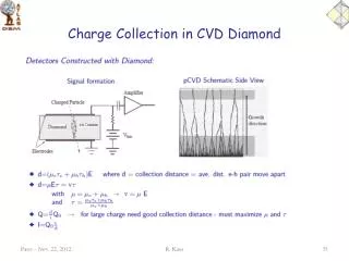
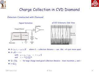
Contents • Low dose rate irradiation of polycrystalline CVD sensors, measure the Charge Collection Distance, CCD vs dose • E64 • Desy7 • Single crystal diamond • IV • Individual spectra • CCD vs HV/time • Summary & outlook C.Grah: Diamond Sensors
Low Dose Rate Irradiation • Usually irradiation in our laboratory is done by: • Irradiation with closest possible distance between source and sensor (typically 2.6 cm) to achieve high dose rate. • Measure the CCD of the sensor in regular time intervals with a reasonable distance to prevent a high double hit rate (typically 7.5cm). • This enables for reproducible measurements on a timescale of several days to get into the 100 Gy range of accumulated dose. • BUT: need of an operator • LOW DOSE RATE IRRADIATION: => automatic CCD measurement at low dose rate, but needs much more time. • Did this at the time of the TAU workshop 2005. C.Grah: Diamond Sensors
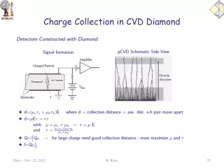
CCD Measurement • Use the high energetic part of a Sr90-β- source => MIP spectrum. Δt = 30min C.Grah: Diamond Sensors
E64 Irradiations • Have done 2 irradiation periods with different dose rates: 29.8. – 5.9. (~7d) 6.9. – 9.11. (~64d) C.Grah: Diamond Sensors
Desy7 and Desy8 • Got these two new samples in Nov. 06. • The samples are 300 μm thick and 12x12 mm in size. • The metallization is 10x10 mm in size divided into 4 pads on one side. • 100 nm Ti + 200 nm Pt + 500 nm Au. • Material selection was with focus on avoiding micro cracks. C.Grah: Diamond Sensors
Desy7 and Desy8 (cont.) • pCVD Diamonds from Freiburg (Fraunhofer IAF) • Main issue from former samples: • micro cracks • IV behavior • CCD performance • CCD vs irradiation • Large part of the measurements were presented by K. Afanaciev. Much better performance than earlier samples. • Issue of signal decreasing with time. FAP7 series C.Grah: Diamond Sensors
Spectra of Desy7 Shortly after switching the high voltage a large signal is measured. Took pedestal as determined by the early measurements and fixed it for the rest. C.Grah: Diamond Sensors
Low Dose Rate Result switching voltage Stable signal! 22.12.05- 11.1.06 C.Grah: Diamond Sensors
BDS7 - IV • Started to investigate a sCVD Diamond. • Got the sample (BDS7) in December from the GSI Darmstadt. • 5 x 5 x 0.318 mm3 ; Cr(50 nm)Au (100 nm) or Ti(30nm)Pt(50nm)Au(100nm) known “breakthrough” C.Grah: Diamond Sensors
Mip signal of BDS7 C.Grah: Diamond Sensors
BDS7 CCD thickness The single crystal diamond shows a high (100%) and stable (t) signal even at low E-field. C.Grah: Diamond Sensors
Summary • Have tested sensors from E6 and IAF (Freiburg) up to highest doses so far in our lab (>250 Gy). • Desy7 and Desy8 show a small but stable signal and did not show any microcrack related problem. • Started to test a single crystal diamond (sCVD) from E6. • Superior efficiency at low E-field and very stable behaviour of the sCVD sample. C.Grah: Diamond Sensors
Outlook • We will get pCVD samples back from Freiburg with annealed (10min@500°C) metallization. Expected this week. • Waiting for new thin samples from Freiburg from a dedicated wafer with reduced nitrogen concentration during growth. • We will have a testbeam period (end of April) at the TU Darmstadt DALINAC (10MeV and ~15Gy/s) and will investigate high dose behavior of diamonds. • sCVD diamonds are interesting but they are not (yet) available on waferlevel. Will follow the development of this technology. C.Grah: Diamond Sensors